GaN vertical heterojunction field-effect transistor with charge compensation voltage-resistant structure

A heterojunction field effect and charge compensation technology, which is applied in the direction of circuits, transistors, electrical components, etc., can solve the limitations of high withstand voltage applications of GaNVHFETs, the breakdown voltage cannot reach the limit of GaN materials, and the high endurance of GaN-based devices cannot be fully utilized. problems such as pressure advantages, to achieve the effect of high process feasibility

Active Publication Date: 2015-12-09
UNIV OF ELECTRONICS SCI & TECH OF CHINA
View PDF3 Cites 11 Cited by
  • Summary
  • Abstract
  • Description
  • Claims
  • Application Information

AI Technical Summary

Problems solved by technology

[0005] For the conventional GaNVHFET structure, the device mainly relies on the p-n junction formed between the p-GaN current blocking layer and the n-GaN buffer layer to withstand the withstand voltage. When the peak electric field in the device reaches the critical electric field or the leakage current reaches the threshold, the n-GaN The width of the depletion region in the buffer layer determines the breakdown voltage of the device. As the thickness of the n-GaN buffer layer increases, the width of the depletion region in the n-GaN also increases during breakdown. However, when n - When the thickness of the GaN buffer layer exceeds a certain value, the width of the depletion region in n-GaN reaches saturation during breakdown, and the breakdown voltage of the device also reaches saturation, which no longer increases with the increase of the thickness of the n-GaN buffer layer , thus limiting the high withstand voltage application of GaNVHFET
At the same time, the vertical electric field intensity in the n-GaN buffer layer will gradually decrease as it moves away from the p-n junction interface between the p-GaN current blocking layer and the n-GaN buffer layer. The integral of the vertical electric field strength along the vertical direction, the decreasing vertical electric field strength makes the breakdown voltage of the device unable to reach the GaN material limit, and cannot fully utilize the high withstand voltage advantages of GaN-based devices

Method used


Image

  • GaN vertical heterojunction field-effect transistor with charge compensation voltage-resistant structure
  • GaN vertical heterojunction field-effect transistor with charge compensation voltage-resistant structure
  • GaN vertical heterojunction field-effect transistor with charge compensation voltage-resistant structure

Examples


Embodiment 1

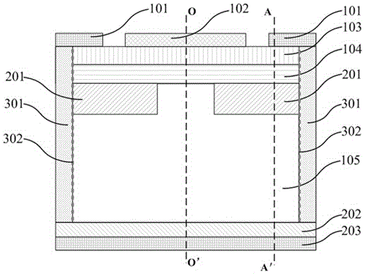
[0028] The main structure of this embodiment, such as image 3 As shown, it includes a barrier layer 103. The upper part of the barrier layer 103 is provided with a source electrode 101 and a gate electrode 102. The source electrode 101 is located on both sides of the device, and the gate electrode 102 is located in the middle part; the lower part is the channel layer 104, the current Barrier layer 201, n-GaN buffer layer 105, n + -GaN substrate 202, drain 203; the center of the current blocking layer 201 has a width of L AP And nested on the upper part of the n-GaN buffer layer 105; the barrier layer 103, the channel layer 104, the current blocking layer 201 and the n-GaN buffer layer 105 are provided with a charge compensation insulating layer 301, which is The layer 301 penetrates the source 101 and n from top to bottom + -GaN substrate 202; its upper surface is connected to source 101, and its lower surface is connected to n + -The surface of the GaN substrate 202 is connect...


PUM


Abstract

The invention discloses a GaN vertical heterojunction field-effect transistor with a charge compensation voltage-resistant structure. The device is characterized in that the GaN vertical heterojunction field-effect transistor with the charge-compensation voltage-resistant structure further comprises a barrier layer, a channel layer, a current barrier layer and a charge compensation insulating layer outside an n-GaN buffer layer, and the fixed charges high in density exist at boundaries between the charge compensation insulating layer and the barrier layer, the channel layer, the current barrier layer and the n-GaN buffer layer, wherein the charge compensation insulating layer is formed by an insulating dielectric medium. The fixed charges high in density exist at boundary between the charge compensation insulating layer and the n-GaN buffer layer, so that in a voltage resistance process, negative charges at the boundary enable inversion of the closer n-GaN buffer layer, a formed p+ column consumes electrons in the n-GaN buffer layer, the buffer layer is enabled to form a p+n super junction structure which is completely exhausted, an electric field in the buffer layer is kept to 3MV/cm in the perpendicular direction after full optimization, and the a device breakdown voltage reaches a voltage-resistant limit of the GaN material.

Description

Technical field [0001] The invention relates to the field of semiconductor high withstand voltage devices, in particular to a vertical gallium nitride-based heterojunction field effect tube with a charge compensation withstand voltage structure. Background technique [0002] GaN-based heterojunction field effect transistors (GaNHeterojunctionField-EffectTransistor, GaNHFET) not only have large forbidden band width, high critical breakdown electric field, high electron saturation speed, good thermal conductivity, radiation resistance and good chemical stability, etc. At the same time, gallium nitride (GaN) material can form a two-dimensional electron gas heterojunction channel with high concentration and high mobility with materials such as aluminum gallium nitride (AlGaN), so it is especially suitable for high-voltage, high-power and high-temperature applications. It is one of the most potential transistors for power electronics applications. [0003] The existing high withstand v...

Claims


Application Information

Patent Timeline
Patent Type & Authority Applications(China)
IPC IPC(8): H01L29/80H01L29/06
CPCH01L29/0611H01L29/802
Inventor 杜江锋刘东白智元潘沛霖于奇
Owner UNIV OF ELECTRONICS SCI & TECH OF CHINA
Why Eureka
Try Eureka