


Quick Research
Generate reliable direction feasibility study reports for your R&D in just a few steps.

Technical Q&A
Discover and master advanced knowledge NOW. Basics, ideas, possibilities, all at once.

Find Solutions
As an expert in R&D theories, this can generate solutions to your technical problems instantly.

Evaluate Feasibility
Analyze your overall solution with one click, know your potential R&D risks in advance.

Monitor Landscape
Get weekly tech updates, stay abreast of the latest tech innovations and key insights.
Display device
A technology for display devices and encapsulation adhesives, applied in organic semiconductor devices, optics, instruments, etc., to achieve the effects of reducing conduction impedance, increasing capacitance value, and increasing storage capacitance
- Summary
- Abstract
- Description
- Claims
- Application Information
AI Technical Summary
Problems solved by technology
Method used
Image


Examples
Embodiment 1
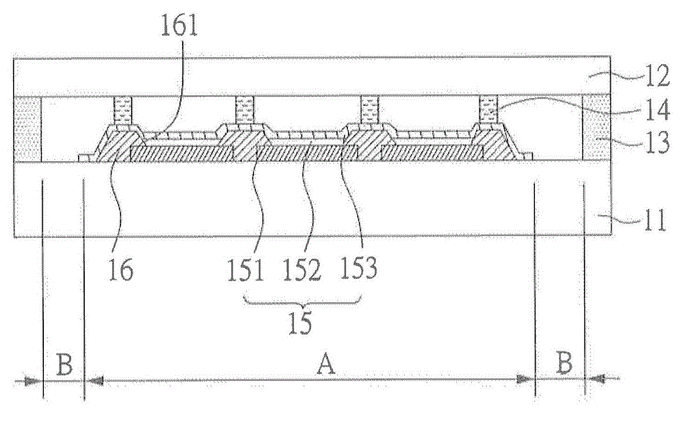
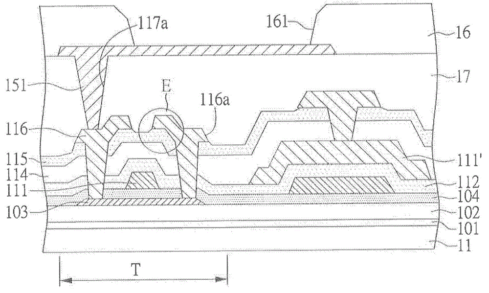
[0048] figure 1 is a schematic cross-sectional view of the organic light emitting diode display device of this embodiment. During the manufacturing process of the OLED display device, a first substrate 11 and a second substrate 12 are firstly provided. Wherein, an OLED unit 11 and a pixel defining layer 16 are disposed on the first substrate 11 , wherein each pixel defining layer 16 is disposed between two adjacent OLED units 15 . At the same time, a plurality of support elements 14 are arranged on the second substrate 12, and an encapsulation glue 13 (in this embodiment, a glass glue) is firstly formed on the edge of the second substrate 12, and the encapsulation glue 13 penetrates the point glue and heating and sintering process to bond on the second substrate 12 . Next, the first substrate 11 and the second substrate 12 are paired, wherein the supporting element 14 on the second substrate 12 corresponds to the area of the pixel defining layer 16 where no pixel opening 1...
Embodiment 2
[0064] like Figure 9 , which is a schematic diagram of the liquid crystal display device of the embodiment. In the manufacturing process of the liquid crystal display device, a first substrate 11 and a second substrate 12 are firstly provided, on which different components (not shown) are arranged respectively. For example, in some embodiments, thin film transistor units are disposed above the first substrate 11, and color filter elements (such as Figure 10shown, wherein the color filter element is not shown in the figure); and in some embodiments, the color filter element and the TFT unit are simultaneously disposed on the first substrate 11 . In addition, one of the first substrate 11 and a second substrate 12 is provided with a plurality of spacers 17, and an encapsulant 13 (in this embodiment, a frame glue) is first formed on the edge of the second substrate 12. ). After the first substrate 11 and the second substrate 12 are assembled, liquid crystal molecules are inj...
PUM
 Abstract
Description
Claims
Application Information
 - R&D Engineer
- R&D Manager
- IP Professional
- Industry Leading Data Capabilities
- Powerful AI technology
- Patent DNA Extraction
Browse by: Latest US Patents, China's latest patents, Technical Efficacy Thesaurus, Application Domain, Technology Topic, Popular Technical Reports.
© 2024 PatSnap. All rights reserved.Legal|Privacy policy|Modern Slavery Act Transparency Statement|Sitemap|About US| Contact US: help@patsnap.com