Processing method of capacitor type MEMS sensor and sensor structure

A processing method and sensor technology, applied to piezoelectric devices/electrostrictive devices, microstructure devices composed of deformable elements, microstructure technology, etc., can solve the problems of increasing investment in fixed assets, difficult quality monitoring, thermal expansion coefficient Large gaps and other issues, to avoid investment in fixed assets and ensure consistency

Active Publication Date: 2015-11-11
GUANGDONG HEWEI INTEGRATED CIRCUIT TECH
View PDF7 Cites 20 Cited by
  • Summary
  • Abstract
  • Description
  • Claims
  • Application Information

AI Technical Summary

Problems solved by technology

[0002] In the prior art, the production of capacitive MEMS sensors usually adopts anodic bonding process. Although the process is relatively mature and simple, the large difference in thermal expansion coefficient between silicon and glass will affect the performance of the device, resulting in a large temperature drift of the sensor.
Moreover, the anodic bonding process is not a standard CMOS process. Glass generally cannot be taped on a CMOS production line because it contains conductive ions, so the process needs to be outsourced, making it difficult to monitor the quality, and investing in corresponding equipment will increase the investm

Method used


Image

  • Processing method of capacitor type MEMS sensor and sensor structure
  • Processing method of capacitor type MEMS sensor and sensor structure
  • Processing method of capacitor type MEMS sensor and sensor structure

Examples


Embodiment Construction

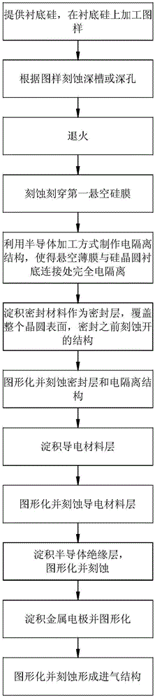
[0052] The technical solutions of the present invention will be further described below in conjunction with the accompanying drawings and through specific implementation methods.

[0053] Such as Figure 1-14 As shown, in the present embodiment, a processing method of a capacitive MEMS sensor according to the present invention comprises the following steps:

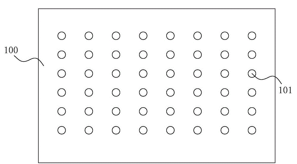
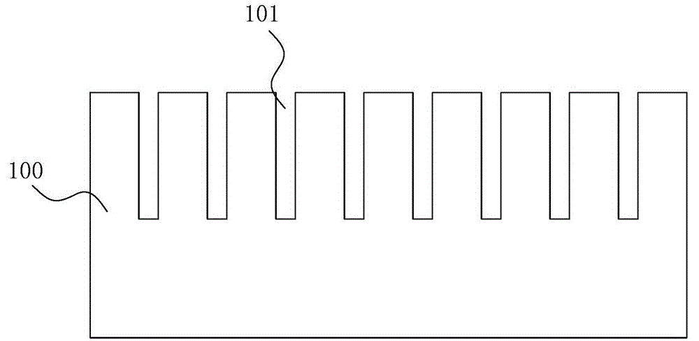
[0054] Step S1, providing a silicon wafer substrate 100, and performing pattern processing on the silicon wafer substrate 100;

[0055] Step S2, etching deep holes 101 on the silicon wafer substrate 100 according to the pattern;

[0056]Step S3, performing annealing treatment on the silicon wafer substrate 100 in a high-temperature oxygen-free environment, so that the silicon atoms on the substrate surface of the silicon wafer 1 are migrated to form a first suspended silicon film 102, a second suspended silicon film 103 and A first cavity 104 located between the first suspended silicon film 102 and the second suspended ...


PUM

PropertyMeasurementUnit
Cross section widthaaaaaaaaaa

Abstract

The invention provides a processing method of a capacitor type MEMS sensor and the capacitor type MEMS sensor. The method adopts a SON (silicon-on-nothing) technology to perform single-faced processing to obtain two layers of silicon films to be used as two electrodes of a capacitor, and measures pressure by utilizing capacitance change brought by shape change after the lower silicon film is pressed. The processing method can be implemented with an IC production line and does not need extra equipment or non-CMOS production line technology, such as anodic bonding. The processing method of the invention facilitates the control of the consistence of the performance of sensors on a whole wafer.

Description

technical field [0001] The invention relates to the technical field of semiconductor equipment processing, in particular to a processing method and sensor structure of a capacitive MEMS sensor. Background technique [0002] In the prior art, the production of capacitive MEMS sensors usually adopts anodic bonding process. Although the process is relatively mature and simple, the large difference in thermal expansion coefficient between silicon and glass will affect the performance of the device, resulting in a large temperature drift of the sensor. Moreover, the anodic bonding process is not a standard CMOS process. Glass generally cannot be taped on a CMOS production line because it contains conductive ions, so the process needs to be outsourced, making it difficult to monitor the quality, and investing in corresponding equipment will increase investment in fixed assets. [0003] In other production methods, a piezoresistive detection structure is formed. Compared with piezo...

Claims


Application Information

Patent Timeline
IPC IPC(8): B81C1/00B81B3/00
Inventor 周志健陈磊邝国华
Owner GUANGDONG HEWEI INTEGRATED CIRCUIT TECH
Why Eureka
Try Eureka