
High-gain class AB operational amplifier circuit

An operational amplifier, high-gain technology, applied in amplifiers, differential amplifiers, DC-coupled DC amplifiers, etc., can solve the problems of low open-loop gain and increased intrinsic gain of operational amplifiers

Active Publication Date: 2015-10-28
CHANGSHA JINGJIA MICROELECTRONICS
View PDF5 Cites 2 Cited by
  • Summary
  • Abstract
  • Description
  • Claims
  • Application Information

AI Technical Summary

Problems solved by technology

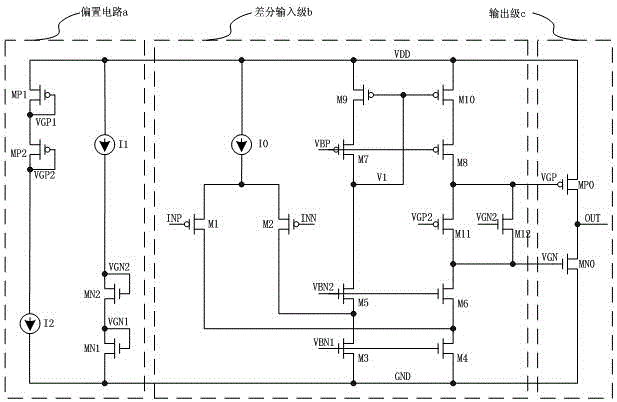
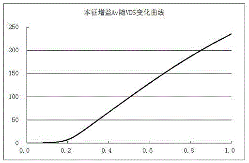
[0007] attached figure 2 It is the change curve of intrinsic gain with VDS voltage when the overdrive voltage of 3.3V NMOS device is 0.2V. It can be seen that the output resistance increases with the increase of VDS, and the intrinsic gain increases; for the above operational amplifier, in order to reduce the static power power consumption, the output stages MN0 and MP0 are weakly turned on, VGN≈VTH NMOS 、VGP≈VDD-VTH PMOS , For the threshold voltage of typical 5V process NMOS and PMOS is about 0.6V, then the VDS voltage of the load transistors M4, M6, M8, M10 is about 0.3V, and they are all in the critical saturation region at this time, and the intrinsic gain is only 34.7, resulting in The open-loop gain of the op amp is low

Method used


Image

  • High-gain class AB operational amplifier circuit
  • High-gain class AB operational amplifier circuit
  • High-gain class AB operational amplifier circuit

Examples


Embodiment Construction

[0014] The structure and working process of a high-gain Class A and B operational amplifier disclosed in the invention will be described in detail below in conjunction with the accompanying drawings.

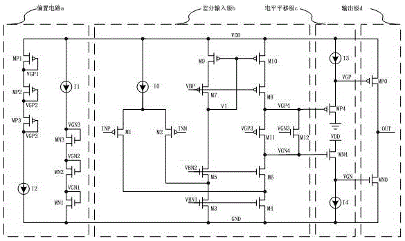
[0015]A specific circuit of a high-gain Class A and B operational amplifier consists of a bias circuit, a differential input stage, a level shift stage and an output stage; the bias circuit (a) consists of 3 NMOS transistors, 3 PMOS transistors and two bias Current composition; the source of NMOS transistor MN1 is grounded, the gate and drain are connected to the source of NMOS transistor MN2; the source node VGN1 of NMOS transistor MN2 is connected to the gate and drain of NMOS transistor MN1, and the gate and drain are connected to NMOS The source of the tube MN3; the source node VGN2 of the NMOS tube MN3 is connected to the gate and drain of the NMOS tube MN2, and the gate and the drain are connected to the gate node VGN3 of the differential input stage NMOS tube M12 and the b...


PUM


Abstract

A class AB operational amplifier is widely applied to integrated circuits due to rail-to-rail output and high load current driving capability. In a conventional structure, a load tube of a differential input stage works in a critical saturation area, leading to low intrinsic gains of the devices and limiting the open-loop gain of the operational amplifier. A level translation circuit is added, so that the devices are separated from the critical saturation area, and the open-loop gain of the operational amplifier is increased greatly. A circuit in the invention consists of a bias circuit, a differential input stage, a level translation stage and an output stage.

Description

technical field [0001] The invention belongs to the field of integrated circuit design and is used for circuits requiring high-gain Class A and B operational amplifiers. Background technique [0002] In integrated circuit design, due to the rail-to-rail output and large load current driving capability of Class A and B operational amplifiers, it is widely used in integrated circuits. In the traditional structure, because the load MOS transistor of the differential input stage works in the critical saturation region, resulting in low intrinsic gain of these devices, which in turn limits the open-loop gain of the op amp; [0003] attached figure 1 It is a traditional class A and B operational amplifier circuit, which is widely used in the output stage of integrated circuit design; the specific circuit is composed of a bias circuit, a differential input stage, and an output stage; the bias circuit (a) consists of 2 NMOS tubes, 2 It consists of a PMOS transistor and two bias cu...

Claims


Application Information

Patent Timeline
Patent Type & Authority Applications(China)
IPC IPC(8): H03F3/45
CPCH03F3/45394H03F2203/45586
Inventor 李亚
Owner CHANGSHA JINGJIA MICROELECTRONICS
Learn More