Longitudinal high-voltage semiconductor device

A semiconductor, high-voltage technology, applied in the direction of semiconductor devices, electrical components, circuits, etc., can solve the problem of surface electric field concentration, and achieve the effect of increasing the lateral withstand voltage length, reducing the surface electric field, and improving the reliability of the device

Inactive Publication Date: 2015-09-09
西安西奈电子科技有限公司
View PDF6 Cites 7 Cited by
  • Summary
  • Abstract
  • Description
  • Claims
  • Application Information

AI Technical Summary

Problems solved by technology

[0003] The ideal breakdown voltage of the device refers to the case where the PN junction is a planar junction, but in the actual process, since the impurity diffuses vertically and also diffuses laterally, the terminal profile that actually forms the PN junction is curved, and the junction surface Bending will lead to surface electric field concentration, which has a great impact on the breakdown characteristics of the PN junction. It is necessary to use the terminal structure to increase the breakdown voltage

Method used


Image

  • Longitudinal high-voltage semiconductor device
  • Longitudinal high-voltage semiconductor device
  • Longitudinal high-voltage semiconductor device

Examples


Embodiment Construction

[0024] In order to make the object, technical solution and advantages of the present invention clearer, the present invention will be further described in detail below in conjunction with the accompanying drawings and embodiments. It should be understood that the specific embodiments described here are only used to explain the present invention, not to limit the present invention.

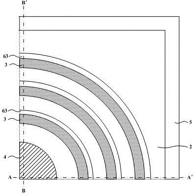
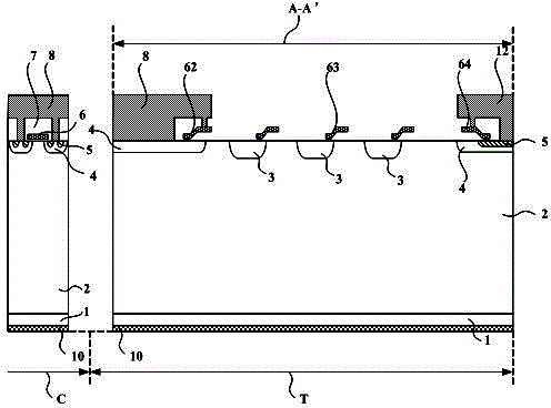
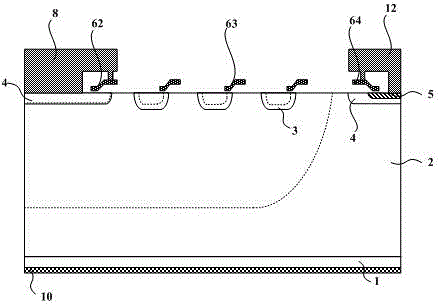
[0025] refer to figure 1 with figure 2 ,Such as figure 1 with figure 2 As shown, a vertical high-voltage semiconductor device includes: N-type doped semiconductor substrate 1, N-type doped epitaxial layer 2, P-type doped well region 3, P-type doped body region 4, high-concentration N-type doped impurity region 5, polysilicon gate 6, second polysilicon field plate 62, third polysilicon field plate 63, fourth polysilicon field plate 64, drain metal electrode 10 and stop ring electrode 12; An N-type doped epitaxial layer 2 is arranged on the N-type doped semiconductor substrate 1, and a P-type d...


PUM


Abstract

The invention discloses a longitudinal high-voltage semiconductor device, comprising an N-type doped semiconductor substrate, an N-type doped epitaxial layer, a P-type doped well region, a P-type dopant region, a high-concentration N-type doped region, a first polycrystalline silicon field plate, a second polycrystalline silicon field plate, a third polycrystalline silicon field plate, a fourth polycrystalline silicon field plate, a drain metal electrode and a stop ring electrode. The device can realize bidirectional exhaust during voltage tolerance, reduces the size of a chip, and lowers the production cost.

Description

technical field [0001] The invention belongs to the technical field of semiconductor power devices and relates to a high-voltage power device, in particular to a vertical high-voltage semiconductor device with a terminal structure of a field limiting ring and a polycrystalline field plate. Background technique [0002] At present, power semiconductor devices are more and more widely used in daily life, production and other fields. Among many power devices, vertical double-diffused metal-oxide-semiconductor field effect transistor (VDMOS: Vertical Double-diffused MOSFET) has the advantages of both bipolar transistors and ordinary MOS devices. Whether it is a switching application or a linear application, VDMOS devices All are ideal power semiconductor devices. Breakdown voltage is one of its important static characteristics. [0003] The ideal breakdown voltage of the device refers to the case where the PN junction is a planar junction, but in the actual process, since the ...

Claims


Application Information

Patent Timeline
Patent Type & Authority Applications(China)
IPC IPC(8): H01L29/78H01L29/06
CPCH01L29/7802H01L29/0607
Inventor 梅冬
Owner 西安西奈电子科技有限公司
Why Eureka
Try Eureka