In cell touch display screen, driving method thereof and display device
A touch display, embedded technology, applied in static indicators, instruments, semiconductor devices, etc., can solve the problems of high production cost, low light transmittance, thick modules, etc.
- Summary
- Abstract
- Description
- Claims
- Application Information
AI Technical Summary
Problems solved by technology
Method used
Image
Examples
Embodiment 1
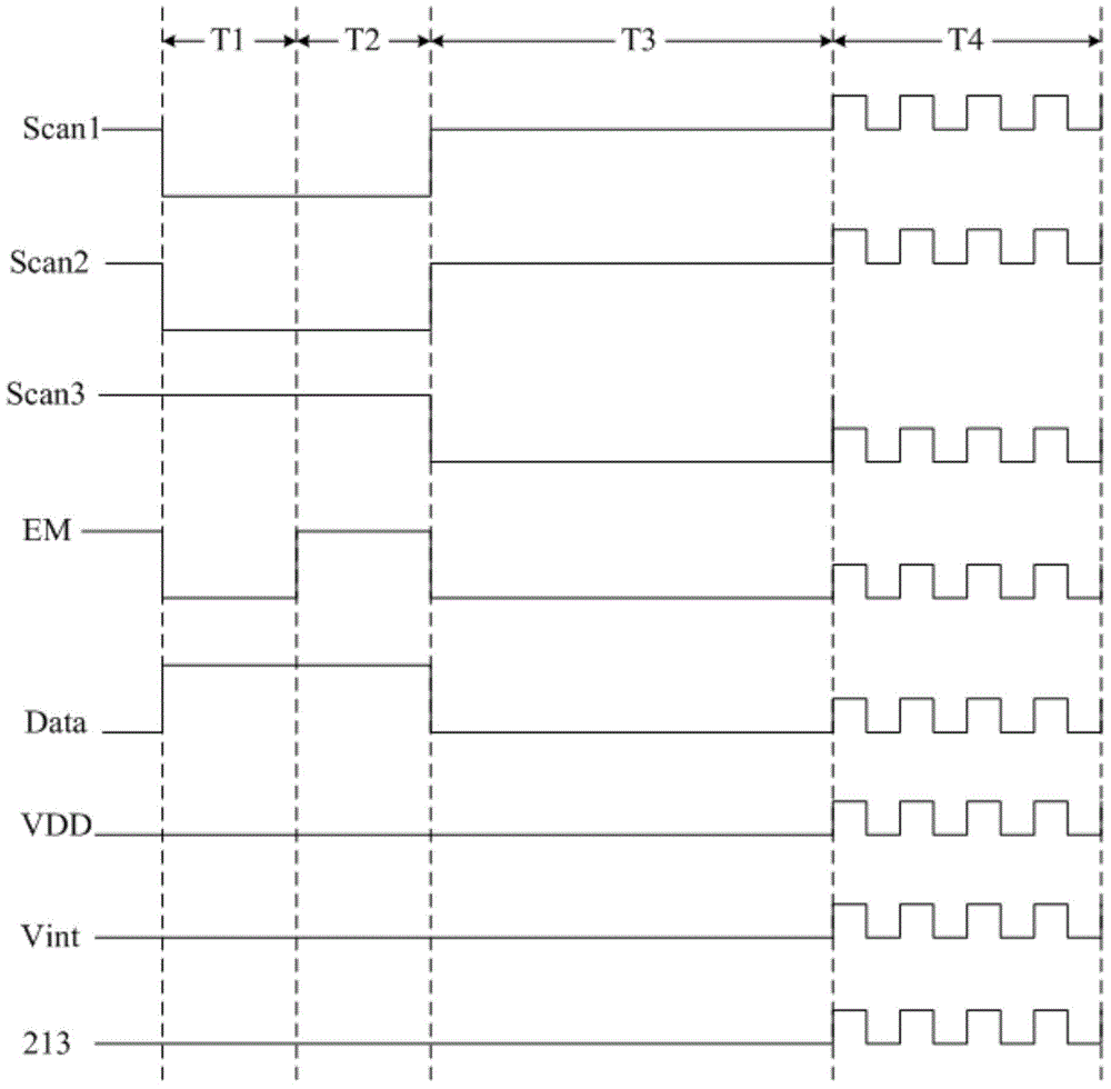
[0098] In the first stage T1 (reset charging stage), Scan1=0, Scan2=0, Scan3=1, EM1=0.
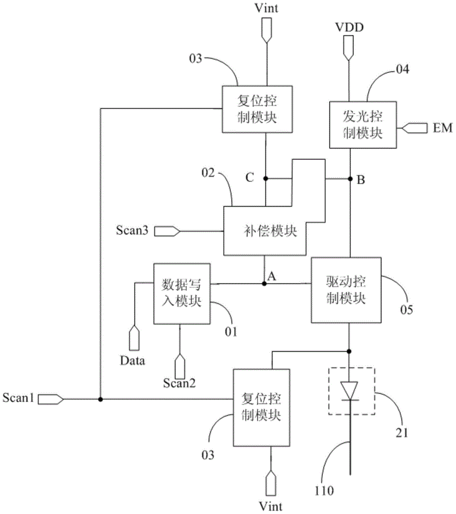
[0099] Such as Figure 5a As shown, the first switching transistor T1, the second switching transistor T2, the third switching transistor T3 and the fifth switching transistor T5 are in the on state, the fourth switching transistor T4 and the driving transistor DT0 are in the off state; the first reference signal terminal VDD The first reference signal is transmitted to the second node B through the turned-on fifth switching transistor T5, so that the potential of the second node B is the potential V of the first reference signal dd , the second reference signal at the second reference signal terminal Vint is transmitted to the third node C through the turned-on second switching transistor T2, so that the potential of the third node C is the potential V of the second reference signal ss , the capacitor C1 starts charging, and the second reference signal at the second reference signal term...
Embodiment 2
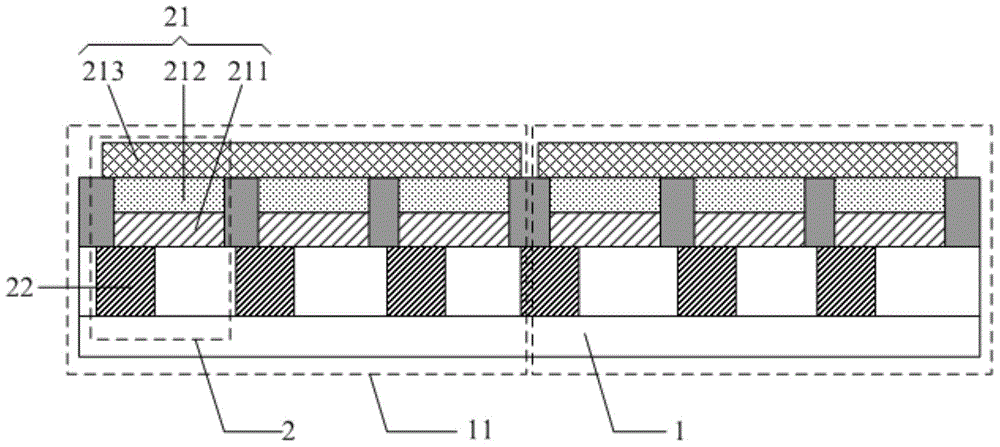
[0130] Take a sub-pixel as an example, such as Figure 8 As shown, the array substrate 1 sequentially includes a buffer layer 221, an active layer 222, a gate insulating layer 223, a gate 224, an interlayer insulating layer 225, a source electrode 226, a drain electrode 227, and a wire 110 arranged on the same layer. layer 228, the anode layer 211 and the cathode connection part 214, the light emitting layer 212, the sub-pixel defining layer 215 surrounding the light emitting layer 212, and the cathode layer 213.
[0131] Wherein, the cathode layer 213 is connected to the cathode connection part 214 through the via hole penetrating the sub-pixel defining layer 215, the anode layer 211 is connected to the drain electrode 227 through the via hole penetrating the planarization layer 228, and the cathode connection part 214 is connected to the drain electrode 227 through the The via hole is connected to the wire 110, the source electrode 226 and the drain electrode 227 are respect...
PUM
 Abstract
Description
Claims
Application Information
 - R&D
- Intellectual Property
- Life Sciences
- Materials
- Tech Scout
- Unparalleled Data Quality
- Higher Quality Content
- 60% Fewer Hallucinations
Browse by: Latest US Patents, China's latest patents, Technical Efficacy Thesaurus, Application Domain, Technology Topic, Popular Technical Reports.
© 2025 PatSnap. All rights reserved.Legal|Privacy policy|Modern Slavery Act Transparency Statement|Sitemap|About US| Contact US: help@patsnap.com


