A pixel circuit, its driving method and related device
A technology for pixel circuits and driving transistors, applied in circuits, electrical components, electrical solid devices, etc., can solve problems such as uneven image brightness, and achieve the effect of improving uniformity
- Summary
- Abstract
- Description
- Claims
- Application Information
AI Technical Summary
Problems solved by technology
Method used
Image
Examples
example 1
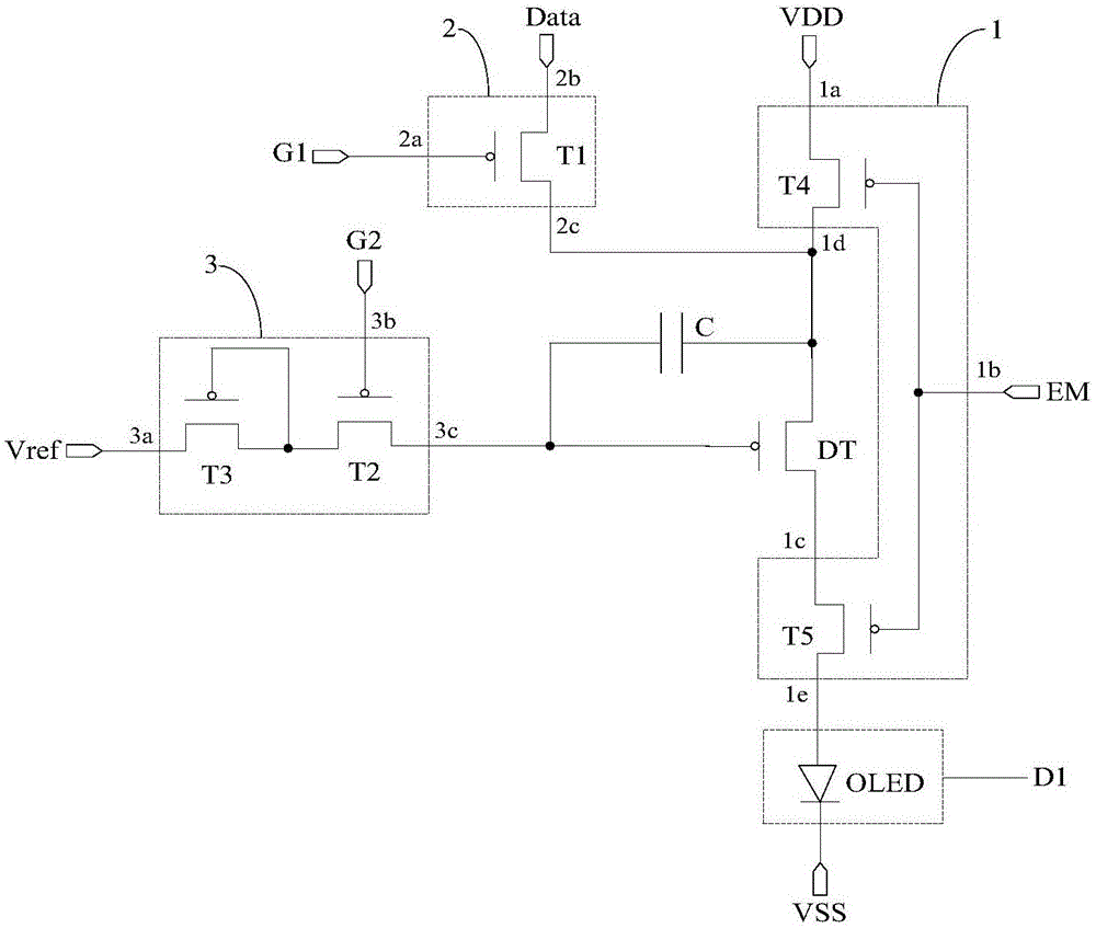
[0074] by Figure 3c The structure of the pixel circuit shown is taken as an example to describe its working process, in which Figure 3c In the pixel circuit shown, the driving transistor is a P-type transistor, and all switching transistors are P-type transistors. Each P-type transistor is turned off under the action of a high level and turned on under the action of a low level; the corresponding input timing diagram is as follows Figure 4a shown. Specifically, choose the Figure 4a Two stages T1 and T2 are shown in the input timing diagram.
[0075] In the T1 stage, G1=0, EM=1. The first switch transistor T1 and the second switch transistor T2 are in an on state, the third switch transistor T3 forms a diode structure, and the fourth switch transistor T4 and the fifth switch transistor T5 are in an off state. Since the first switch transistor T1 is turned on, the voltage of the first node A is the voltage V of the data signal Data Data , since the second switch transis...
example 2
[0078] by Figure 3d The structure of the pixel circuit shown is taken as an example to describe its working process, in which Figure 3d In the pixel circuit shown, the driving transistor and the third switching transistor are P-type transistors, and the other switching transistors are N-type transistors, and each N-type transistor is turned on under the action of a high level, and is turned off under the action of a low level; corresponding The input timing diagram of Figure 4b shown. Specifically, choose the Figure 4b Two stages T1 and T2 are shown in the input timing diagram.
[0079] In the T1 stage, G1=1, EM=0. The first switch transistor T1 and the second switch transistor T2 are in an on state, the third switch transistor T3 forms a diode structure, and the fourth switch transistor T4 and the fifth switch transistor T5 are in an off state. Since the first switch transistor T1 is turned on, the voltage of the first node A is the voltage V of the data signal Data ...
PUM
 Abstract
Description
Claims
Application Information
 - R&D Engineer
- R&D Manager
- IP Professional
- Industry Leading Data Capabilities
- Powerful AI technology
- Patent DNA Extraction
Browse by: Latest US Patents, China's latest patents, Technical Efficacy Thesaurus, Application Domain, Technology Topic, Popular Technical Reports.
© 2024 PatSnap. All rights reserved.Legal|Privacy policy|Modern Slavery Act Transparency Statement|Sitemap|About US| Contact US: help@patsnap.com


