Surface-enhanced raman scattering base on basis of special-material superabsorbers and preparation method thereof
A surface-enhanced Raman and metamaterial technology, applied in the fields of micro-nano photonics and bioanalytical chemistry, can solve the problem that the optical response wavelength range of broad-spectrum one-dimensional metamaterials is not enough to meet the practical application of broad-spectrum Raman scattering spectroscopic analysis, wide-spectrum The problems of unsatisfied spectral optical response, expensive and complex fabrication technology, etc., can simplify multiple vibration and rotation modes, save detection time and cost, and enhance the intensity of Raman scattering signals.
- Summary
- Abstract
- Description
- Claims
- Application Information
AI Technical Summary
Problems solved by technology
Method used
Image
Examples
Embodiment 1
[0039] Example 1: Glass substrate / chrome adhesion layer / continuous silver film / SiO 2 Dielectric layer / gold nanoparticle layer
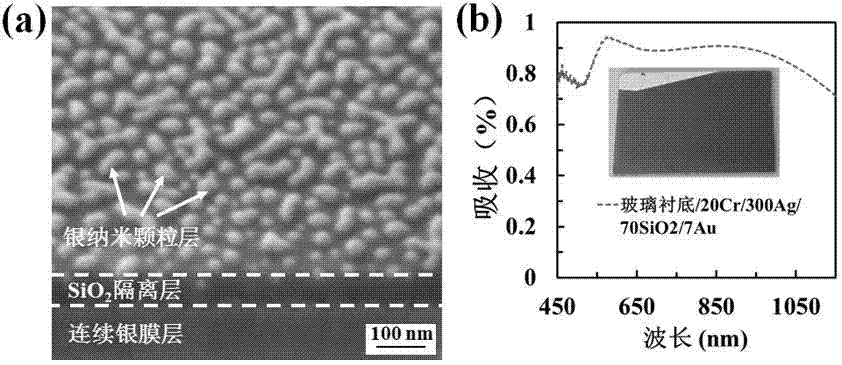
[0040] (1) With the glass substrate as the substrate, a 20 nm thick chromium film is deposited in the electron beam evaporation equipment, which can increase the adsorption force between the glass substrate and the upper continuous metal film, and continue to evaporate a 300 nm thick chromium film on the chromium film. Flat continuous Ag film on which 70 nm SiO is evaporated 2 Membrane as an isolation layer.
[0041] (2) In Ag / SiO 2 A gold film with a nominal thickness of 7 nm was continuously evaporated on the film. Since the thickness was less than the permeation threshold of the gold material, the top gold film self-assembled into gold nanoparticles separated from each other, such as figure 2 (a) shown.
[0042] (3) The prepared structure can achieve more than 70% optical absorption in the visible-near-infrared wavelength range from 450 ...
Embodiment 2
[0043] Example 2: Quartz substrate / silver nanoparticle layer / SiO 2 Dielectric layer / continuous silver film
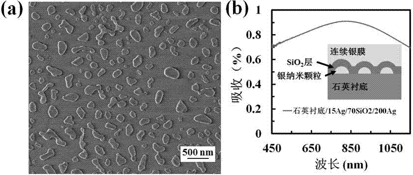
[0044] (1) With the quartz substrate as the substrate, a silver film with a nominal thickness of 15 nm is first plated in a magnetron sputtering equipment. Since the thickness of the silver film is much greater than the permeation threshold, a heat treatment process is required to heat the silver film in vacuum for 500 ℃ for 1 hour to obtain discontinuous silver nanoparticles, such as image 3 (a) shown.
[0045] (2) E-beam evaporation of 70 nm SiO on the silver nanoparticle layer 2 The conceptual diagram of the structure of the inverted metamaterial superabsorber formed by the isolation layer and the 200 nm continuous silver film is shown in image 3 (b) is shown in the inset.
[0046] (3) image 3 (b) is the measured optical absorption spectrum. The results show that the three-layer structure achieves more than 70% optical superabsorption from visible light...
Embodiment 3
[0047] Embodiment 3: glass substrate / continuous silver film / al 2 o 3 Dielectric layer / primary silver nanoparticle layer / secondary silver nanoparticle layer
[0048] (1) With the glass substrate as the substrate, a flat and continuous Ag film with a thickness of 300 nm is plated in a magnetron sputtering device, and 90 nm Al is evaporated with an electron beam on top of it. 2 o 3 membrane.
[0049] (2) In Ag / Al 2 o 3 Continue to sputter a silver film with a nominal thickness of 16 nm on the film. Since the thickness is greater than the permeation threshold of the silver material, the sample needs to undergo a vacuum heat treatment process at 200 ° C for one hour, so that the initial morphology of the top-layer connected silver film is successfully transformed into Silver nanoparticles separated from each other.
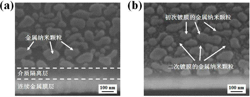
[0050] (3) On the basis of the structure prepared by the initial coating, continue to sputter a silver film with a nominal thickness of 4 nm. Since this th...
PUM
| Property | Measurement | Unit |
|---|---|---|
| Thickness | aaaaa | aaaaa |
| Thickness | aaaaa | aaaaa |
| Thickness | aaaaa | aaaaa |
Abstract
Description
Claims
Application Information
 - R&D Engineer
- R&D Manager
- IP Professional
- Industry Leading Data Capabilities
- Powerful AI technology
- Patent DNA Extraction
Browse by: Latest US Patents, China's latest patents, Technical Efficacy Thesaurus, Application Domain, Technology Topic, Popular Technical Reports.
© 2024 PatSnap. All rights reserved.Legal|Privacy policy|Modern Slavery Act Transparency Statement|Sitemap|About US| Contact US: help@patsnap.com


