Method for electroplating surface of circuit board

A technology for circuit boards and electroplating areas, used in printed circuits, printed circuit manufacturing, and removal of conductive materials by chemical/electrolytic methods. The number of bits, the effect of improving the alignment accuracy, good filling and protection

Active Publication Date: 2015-06-03
SHENNAN CIRCUITS
View PDF5 Cites 4 Cited by
  • Summary
  • Abstract
  • Description
  • Claims
  • Application Information

AI Technical Summary

Problems solved by technology

[0010] The embodiment of the present invention provides a method for electroplating gold on the surface of a circuit board to solve defects such as gold plating penetration, unclean etching, and gold-plated area collapse in the existing gold-plating process before graphics and short circuits in the local gold-plating process of the thin copper method. Risk and defects that increase alignment times for processing boards with high-density wiring and high-precision dimension requirements

Method used


Image

  • Method for electroplating surface of circuit board
  • Method for electroplating surface of circuit board
  • Method for electroplating surface of circuit board

Examples


Embodiment Construction

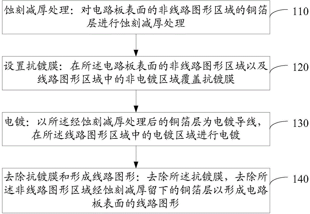
[0023] An embodiment of the present invention provides a method for electroplating the surface of a circuit board to solve the defects of the existing pre-pattern electroplating process, such as gold plating penetration, unclean etching, and collapse of the gold plating area, so as to be used for processing circuits with high density and high precision. board size requirements. The gold plating in the present invention includes electroplated gold, nickel gold, nickel palladium gold and the like.

[0024] In order to enable those skilled in the art to better understand the solutions of the present invention, the following will clearly and completely describe the technical solutions in the embodiments of the present invention in conjunction with the drawings in the embodiments of the present invention. Obviously, the described embodiments are only It is an embodiment of a part of the present invention, but not all embodiments. Based on the embodiments of the present invention, ...


PUM

PropertyMeasurementUnit
thicknessaaaaaaaaaa

Abstract

The invention discloses a method for electroplating the surface of a circuit board. The method comprises the following steps: performing etching thickness reduction treatment, namely performing etching thickness reduction treatment on a copper foil layer of a non-line graph region on the surface of the circuit board; arranging an electroplated film, namely covering the non-line graph region and a non-electroplated area in a line graph region on the surface of the circuit board with the electroplated film; performing electroplating, namely performing electroplating on the electroplated area in the line graph region by taking the copper foil layer subjected to the etching thickness reduction treatment as an electroplating wire; removing the electroplated film and forming a line graph, namely removing the electroplated film, and removing the copper foil layer left by etching thickness reduction in the non-line graph region to form the line graph on the surface of the circuit board. According to the technical scheme, the shortcomings of gold plating permeation, incomplete etching, collapse of a gold-plated region, short-circuit risk or the like of a conventional gold plating process are overcome; the method can be used for machining a circuit board with the requirements of high-density line and high-accuracy dimension.

Description

technical field [0001] The invention relates to the technical field of circuit boards, in particular to a method for surface electroplating of circuit boards. Background technique [0002] In the circuit board processing technology, there is a process of gold-plating the surface pad (PAD) or line of the circuit board to play the role of wear resistance and gold wire. [0003] The gold-plating process is usually realized by the method of gold-plating before graphics, that is, before making surface circuit graphics, use a large copper surface as a gold-plated wire, cover other areas with a dry film, and gold-plate the area that needs to be gold-plated. However, the above-mentioned method of pre-pattern gold plating has the following defects, which cannot meet the increasingly higher gold plating requirements. [0004] a. Gold plating, plating and etching are not clean. In the non-gold-plated area covered by the dry film, because the bonding force between the dry film and the...

Claims


Application Information

Patent Timeline
Patent Type & Authority Applications(China)
IPC IPC(8): H05K3/18C25D5/02
CPCC25D5/022H05K3/06H05K3/18
Inventor 沙雷崔荣刘宝林
Owner SHENNAN CIRCUITS
Why Eureka
Try Eureka