A packaging process suitable for small batch circuits
A packaging process, small batch technology, applied in the manufacturing of circuits, electrical components, semiconductor/solid-state devices, etc., can solve the problems of circuit or chip damage, poor impact resistance, strength reduction, etc., to improve the yield, anti-vibration shock The effect of good performance and quality improvement
- Summary
- Abstract
- Description
- Claims
- Application Information
AI Technical Summary
Problems solved by technology
Method used
Image
Examples
Embodiment Construction
[0027] The present invention will be further described below in conjunction with the accompanying drawings and specific embodiments.
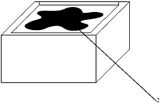
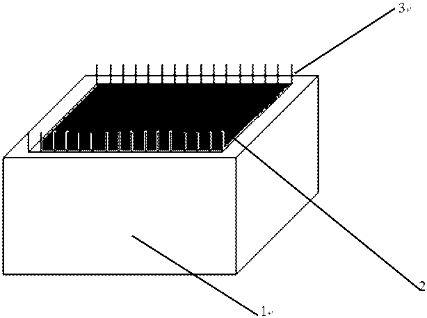
[0028] image 3 It is the circuit to be packaged in the embodiment. When the circuit will be used in an environment of minus 55 degrees Celsius to 125 degrees Celsius, it needs to be resistant to vibration and shock. Packaging not only improves its confidentiality, but also increases its mechanical strength.
[0029] The packaging, aging and testing of the circuit are carried out at the same time, and the whole process is as follows:
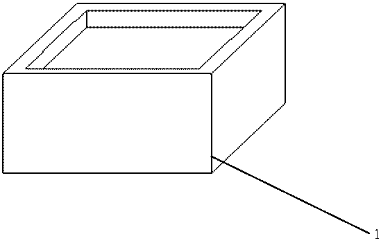
[0030] (a) Pour the curing agent into the mold first, then put the circuit into the mold, and let the circuit immerse in the curing agent;
[0031] (b) Raise the mold together with the circuit from the room temperature S1°C to the specified high temperature S2°C;
[0032] (c) Make the circuit work at S2°C for t1 minutes, keep it for t2 minutes after power off, repeat the process of t1 and t2 many times, and th...
PUM
 Abstract
Description
Claims
Application Information
 - R&D Engineer
- R&D Manager
- IP Professional
- Industry Leading Data Capabilities
- Powerful AI technology
- Patent DNA Extraction
Browse by: Latest US Patents, China's latest patents, Technical Efficacy Thesaurus, Application Domain, Technology Topic, Popular Technical Reports.
© 2024 PatSnap. All rights reserved.Legal|Privacy policy|Modern Slavery Act Transparency Statement|Sitemap|About US| Contact US: help@patsnap.com


