Supercharge Your Innovation With Domain-Expert AI Agents!

Wet etching method of planar optical waveguide and manufacturing method

A planar optical waveguide and wet etching technology, applied in the directions of light guides, optics, optical components, etc., can solve the problems of low manufacturing efficiency of planar optical waveguides, high manufacturing cost of planar optical waveguides, slow etching rate, etc., so as to avoid etching. Insufficient and excessive etching, efficient etching, and the effect of improving product yield

Active Publication Date: 2015-05-20
SOLOREIN TECH
View PDF5 Cites 3 Cited by
  • Summary
  • Abstract
  • Description
  • Claims
  • Application Information

AI Technical Summary

Problems solved by technology

However, the use of a large amount of etching reagents leads to high manufacturing costs of planar optical waveguides, and the etching rate is slow, resulting in low production efficiency of planar optical waveguides.

Method used


Image

  • Wet etching method of planar optical waveguide and manufacturing method
  • Wet etching method of planar optical waveguide and manufacturing method
  • Wet etching method of planar optical waveguide and manufacturing method

Examples


Embodiment Construction

[0030] The following will clearly and completely describe the technical solutions in the embodiments of the present invention with reference to the accompanying drawings in the embodiments of the present invention. Obviously, the described embodiments are only some, not all, embodiments of the present invention. Based on the embodiments of the present invention, all other embodiments obtained by persons of ordinary skill in the art without making creative efforts belong to the protection scope of the present invention.

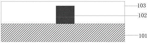
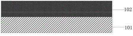
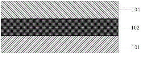
[0031] The embodiment of the present application provides a wet etching method for a planar optical waveguide, refer to figure 2 , figure 2 A schematic flow diagram of a wet etching method for a planar optical waveguide provided in an embodiment of the present application, the flow includes:

[0032] Step S31: forming a patterned photoresist layer on the surface of the metal layer as a first mask layer.

[0033] In this step, the metal layer may be chromiu...


PUM


Abstract

The invention discloses a wet etching method of a planar optical waveguide. The method is used for quickly etching a metal layer on the surface of a substrate. The wet etching method comprises the following steps: forming a patterned photoresist layer on the surface of the metal layer to serve as a first mask layer; horizontally placing the substrate with the metal face facing upwards and soaking in etching solution to etch the metal layer so as to form the patterned metal layer, wherein the etching solution moves relative to the substrate in the etching process; removing the first mask layer after the etching is completed. The substrate is etched by using the wet etching method, so the cost is low and the working efficiency is high. The invention also discloses a manufacturing method of the planar optical waveguide. By using the method, the manufacturing efficiency of the optical waveguide is improved and the cost is reduced.

Description

technical field [0001] The invention relates to the technical field of optical communication equipment manufacturing, in particular to a wet etching method and a manufacturing method of a planar optical waveguide. Background technique [0002] Optical communication is a communication method using light as the medium. It has the advantages of wide transmission frequency bandwidth, large communication capacity, and strong anti-electromagnetic interference ability. It is gradually replacing traditional communication methods. Therefore, the manufacturing of optical communication equipment is also showing vigorous development. situation. [0003] Planar optical waveguide devices are widely used in optical modulators, optical switches, optical power splitters, optical couplers, wavelength division multiplexers, optical filters, polarization divisions, etc. due to their small size, high integration, and good reliability. In optical products such as beamers and microlenses, it has ...

Claims


Application Information

Patent Timeline
IPC IPC(8): G02B6/126C23F1/02
CPCC23F1/02G02B6/136
Inventor 向舟翊李朝阳
Owner SOLOREIN TECH
Features
  • R&D
  • Intellectual Property
  • Life Sciences
  • Materials
  • Tech Scout
  • Unparalleled Data Quality
  • Higher Quality Content
  • 60% Fewer Hallucinations
Learn More