MAX phase ceramic material welding method
A technology of ceramic materials and welding methods, which is applied in the welding field of MAX-phase ceramic materials, can solve the problems of reduced efficiency, high equipment requirements, and increased costs, and achieve the effects of enhanced bending strength, high flexibility, and short welding cycles
- Summary
- Abstract
- Description
- Claims
- Application Information
AI Technical Summary
Problems solved by technology
Method used
Image
Examples
Embodiment 1
[0031] In this embodiment, both the first MAX phase ceramic material 1 and the second MAX phase ceramic material 2 are Ti 3 SiC 2 bulk material, for two Ti 3 SiC 2 The material is welded, the specific method is as follows:
[0032] (1) Put two pieces of Ti 3 SiC 2 After grinding and polishing the surfaces to be welded of materials 1 and 2, wash them with acetone and deionized water;
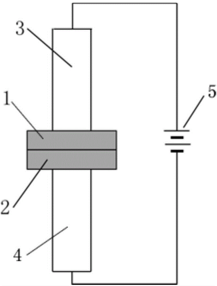
[0033] (2) if figure 1 As shown, the two Ti 3 SiC 2 The surfaces of the materials to be welded are aligned and contacted together, and the two Ti 3 SiC 2 The materials are respectively connected with the graphite upper electrode 3 and the graphite lower electrode 4, the power supply 5, the graphite upper electrode 3, two pieces of Ti 3 SiC 2 Materials 1 and 2 and graphite lower electrode 4 form a closed loop;
[0034](3) Through graphite electrodes 3 and 4 on two pieces of Ti 3 SiC 2 Apply a pressure of 13MPa on materials 1 and 2;
[0035] (4) Apply current to the whole system, Ti ...
Embodiment 2
[0039] In this embodiment, both the first MAX phase ceramic material 1 and the second MAX phase ceramic material 2 are Ti 3 SiC 2 bulk material, for two Ti 3 SiC 2 The material is welded, the specific method is basically the same as that described in Example 1, the difference is that in step (3), graphite electrodes 3 and 4 are used on two Ti 3 SiC 2 A pressure of 1 MPa is applied to materials 1 and 2; in step (4), the current intensity is loaded to 2.2KA and the current is stopped; the welding process takes 7 minutes.
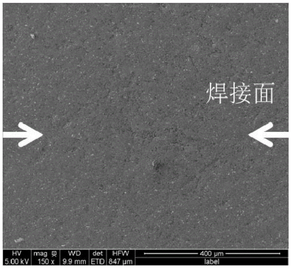
[0040] Figure 4 is the ti 3 SiC 2 Scanning electron microscope (SEM) photograph of the interface cross-section of the material after welding. It can be seen from the figure that the two Ti 3 SiC 2 The material is connected as one, there is no weld seam at the interface, and there is no interface.
Embodiment 3
[0042] In this embodiment, both the first MAX phase ceramic material 1 and the second MAX phase ceramic material 2 are Ti 3 SiC 2 bulk material, for two Ti 3 SiC 2 The material is welded, the specific method is basically the same as that described in Example 1, the difference is that in step (3), graphite electrodes 3 and 4 are used on two Ti 3 SiC 2 A pressure of 5 MPa is applied to materials 1 and 2; in step (4), the current is stopped after the current intensity reaches 2.5KA; the welding process takes 6 minutes.
[0043] Figure 5 is the ti 3 SiC 2 Scanning electron microscope (SEM) photograph of the interface cross-section of the material after welding. It can be seen from the figure that the two Ti 3 SiC 2 The material is connected as one, there is no weld seam at the interface, and there is no interface.
PUM
 Abstract
Description
Claims
Application Information
 - R&D
- Intellectual Property
- Life Sciences
- Materials
- Tech Scout
- Unparalleled Data Quality
- Higher Quality Content
- 60% Fewer Hallucinations
Browse by: Latest US Patents, China's latest patents, Technical Efficacy Thesaurus, Application Domain, Technology Topic, Popular Technical Reports.
© 2025 PatSnap. All rights reserved.Legal|Privacy policy|Modern Slavery Act Transparency Statement|Sitemap|About US| Contact US: help@patsnap.com


