Transistor-Eingangsanpassung mit Transformator

A technology of transformers and power transistors, applied in the field of input matching, which can solve problems such as not suppressing the maximum available gain at low frequencies

Active Publication Date: 2015-05-13
沃孚半导体公司
View PDF5 Cites 0 Cited by
  • Summary
  • Abstract
  • Description
  • Claims
  • Application Information

AI Technical Summary

Problems solved by technology

However, this implementation does not inhibit the maximum available gain at low frequencies, so high gain at low frequencies causes stability, robustness, and linearity correction issues when the source and / or load are mismatched to 50 ohms

Method used


Image

  • Transistor-Eingangsanpassung mit Transformator
  • Transistor-Eingangsanpassung mit Transformator
  • Transistor-Eingangsanpassung mit Transformator

Examples


Embodiment Construction

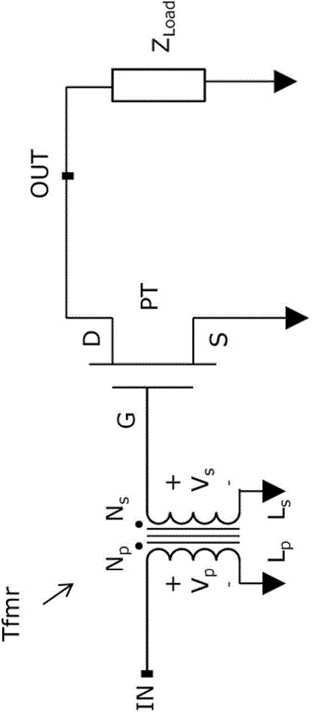
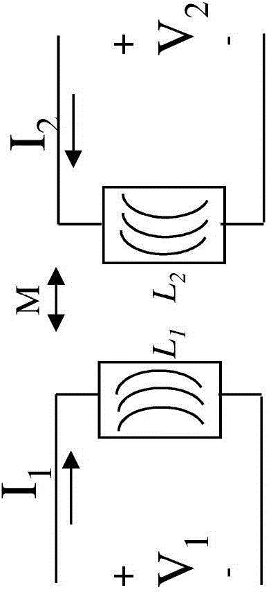
[0022] According to embodiments described herein, a transformer principle is used at the input of the RF power transistor to match the input impedance and create a high pass frequency response that suppresses low frequency gain. In a transformer, a changing alternating current in the primary (P) winding produces a changing magnetic flux which induces a changing voltage in the secondary (S) winding. At low frequency and DC, the package's input lead is isolated from the input (gate) of the RF power transistor by a transformer that operates effectively only at high frequencies, so that the transformer forms a high-pass network. This configuration effectively reduces and suppresses both the maximum available gain and the forward voltage (S21 ) gain hit at low frequencies. The impedance at the input leads of the package no longer depends on the input impedance of the RF power transistor, but on the electrical characteristics of the primary winding.

[0023] By effectively suppress...


PUM


Abstract

An RF power transistor package includes an input lead, an output lead, and an RF power transistor having a gate, a drain and a defined gain over an RF frequency range for which the RF power transistor is configured to operate. The RF power transistor package further includes a transformer electrically isolating and inductively coupling the gate of the RF power transistor to the input lead. The transformer is configured to block signals below the RF frequency range of the RF power transistor and pass signals within the RF frequency range of the RF power transistor. The RF power transistor package also includes a DC feed terminal for providing DC bias to the gate of the RF power transistor.

Description

technical field [0001] This application relates to RF power transistors, and more particularly to input matching for RF power transistors. Background technique [0002] High power RF transistors such as LDMOS (Laterally Diffused Metal Oxide Semiconductor) transistors have input and output impedances (high Q impedance) significantly below 50 ohms, whereas normal RF circuits must be matched to 50 ohms. In order to achieve impedance matching to 50 ohms, RF transistors are usually designed with matching circuits integrated in the packaged transistor at the input and output of the transistor. The matching network helps reduce the Q of the packaged transistor, making it easier to match to 50 ohms. Typically, impedance improvement can only be achieved within a narrow frequency range. In addition, matching networks help shape the frequency response of transistors and amplifiers so that there is high gain at the desired operating frequency while suppressing gain outside that freque...

Claims


Application Information

Patent Timeline
Patent Type & Authority Applications(China)
IPC IPC(8): H01L23/48H01L23/52H03F3/195
CPCH01L24/49H01L2224/48091H01L2224/48137H01L2224/4903H01L2224/49111H01L2224/49175H01L2924/3011H01L2924/30111H01L2924/181H01L2924/00014H01L2924/12042H01L23/66H01L2223/6611H01L2223/6644H01L2223/665H03F3/193H03F2200/534H01L24/48H01L27/0629H01L2924/00H01L2224/45099H01L2224/05599
Inventor M·玛贝尔E·哈希莫托
Owner 沃孚半导体公司
Why Eureka
Try Eureka