Polarizer and manufacturing method thereof, display panel and display device
A manufacturing method and technology of polarizers, applied in the field of optics, can solve problems such as infeasibility, inability to obtain better reproducibility, troubles with the accuracy of the error range of sampling position instruments, etc., and achieve the effect that is not easy to warp
- Summary
- Abstract
- Description
- Claims
- Application Information
AI Technical Summary
Problems solved by technology
Method used
Image
Examples
Embodiment 1
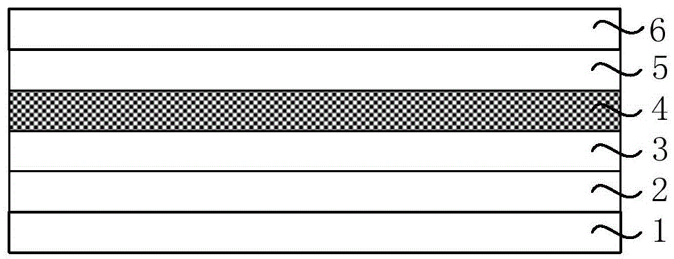
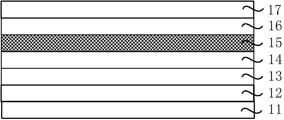
[0046] Please refer to figure 2 , figure 2 It is a schematic cross-sectional view of a polarizer provided in Embodiment 1 of the present invention.
[0047] The polarizer provided in Embodiment 1 of the present invention includes: a first light-transmitting layer 16; a second light-transmitting layer 13, disposed opposite to the first light-transmitting layer 16; a polarizing layer 15, disposed on the first light-transmitting layer Between the layer 16 and the second light-transmitting layer 13; the second organic layer 14 is arranged between the second light-transmitting layer 13 and the polarizing layer 15; wherein, the contraction of the second organic layer 14 The stress direction is perpendicular to the contraction stress direction of the polarizing layer 15 .
[0048] Wherein, the thicknesses of the first transparent layer 16 and the second transparent layer 13 are both 1-40um, and 25um is taken as an example in this embodiment. Of course, the thickness of the first ...
Embodiment 2
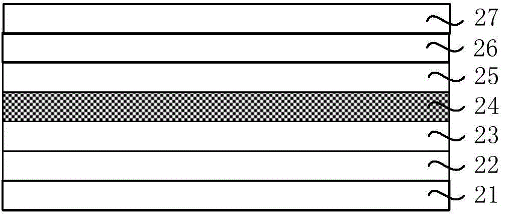
[0054] Please refer to image 3 , image 3 It is a schematic cross-sectional view of a polarizer provided in Embodiment 2 of the present invention.
[0055] The polarizer provided in Embodiment 2 of the present invention includes: a first light-transmitting layer 26; a second light-transmitting layer 23, arranged opposite to the first light-transmitting layer 26; a polarizing layer 24, arranged on the first light-transmitting layer 26 Between the layer 26 and the second light-transmitting layer 23; the first organic layer 25 is arranged between the first light-transmitting layer 26 and the polarizing layer 24; wherein, the contraction of the first organic layer 25 The stress direction is perpendicular to the shrinkage stress direction of the polarizing layer 24, please refer to Figure 4 , Figure 4 It is a schematic diagram of shrinkage stress of a polarizer provided in Embodiment 2 of the present invention. like Figure 4 As shown, the direction of the shrinkage stress ...
Embodiment 3
[0062] Please refer to Figure 5 , Figure 5 is a schematic cross-sectional view of a display panel including the polarizer provided in Embodiment 3 of the present invention. The display panel provided by the third embodiment of the present invention includes: a first substrate 32; a second substrate 36, which is arranged opposite to the first substrate 32; a liquid crystal layer 35, which is encapsulated on the first substrate 32 and the second substrate 36 Between; the first polarizer 31, arranged on the surface of the first substrate 32 away from the second substrate 36 side; the second polarizer 37, arranged on the second substrate 36 away from the first substrate 32; wherein, the direction of the shrinkage stress of the first polarizer 31 is the same as the direction of the shrinkage stress of the second polarizer 37.
[0063] The display panel provided by Embodiment 3 of the present invention further includes spacer columns 33 for maintaining the distance between the t...
PUM
 Abstract
Description
Claims
Application Information
 - R&D
- Intellectual Property
- Life Sciences
- Materials
- Tech Scout
- Unparalleled Data Quality
- Higher Quality Content
- 60% Fewer Hallucinations
Browse by: Latest US Patents, China's latest patents, Technical Efficacy Thesaurus, Application Domain, Technology Topic, Popular Technical Reports.
© 2025 PatSnap. All rights reserved.Legal|Privacy policy|Modern Slavery Act Transparency Statement|Sitemap|About US| Contact US: help@patsnap.com


