
A method for reducing the k value of the dielectric material between vias in the back-end copper interconnection process

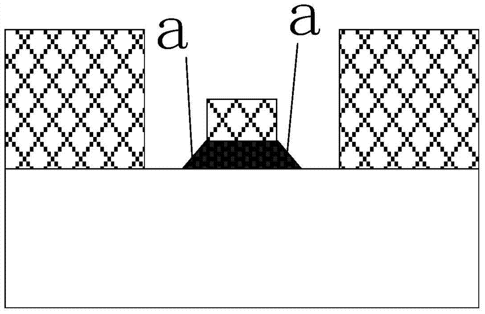
A dielectric material and copper interconnection technology, which is applied in the manufacture of electrical components, electrical solid-state devices, semiconductor/solid-state devices, etc. The effect of height and angle increases

Active Publication Date: 2017-08-22
SHANGHAI HUALI MICROELECTRONICS CORP
View PDF4 Cites 0 Cited by
  • Summary
  • Abstract
  • Description
  • Claims
  • Application Information

AI Technical Summary

Problems solved by technology

However, since the bottom of the porous low-k dielectric material has a silicon oxide layer and a nitrogen-doped silicon carbide layer, and the K value of the silicon oxide material is about 3.9, the K value of the nitrogen-doped silicon carbide layer is about 5.9, and the silicon oxide layer and The material of the nitrogen-doped silicon carbide layer can be considered as a dielectric material, so it will further increase the overall K value of the dielectric material between the vias.

Method used


Image

  • A method for reducing the k value of the dielectric material between vias in the back-end copper interconnection process
  • A method for reducing the k value of the dielectric material between vias in the back-end copper interconnection process
  • A method for reducing the k value of the dielectric material between vias in the back-end copper interconnection process

Examples


Embodiment Construction

[0027] In order to make the content of the present invention clearer and easier to understand, the content of the present invention will be further described below in conjunction with the accompanying drawings. Of course, the present invention is not limited to this specific embodiment, and general replacements known to those skilled in the art are also covered within the protection scope of the present invention.

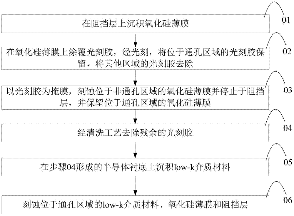
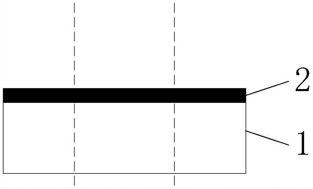
[0028] The following will be combined with Figure 2-8 The method for reducing the K value of the dielectric material between vias of the present invention will be further described in detail with specific embodiments. in, figure 2 It is a schematic flow chart of a method for reducing the K value of the dielectric material between vias according to a preferred embodiment of the present invention, image 3 It is a schematic structural diagram of a semiconductor substrate of a preferred embodiment of the present invention, Figure 4-8 It is a schematic diagram of...


PUM

PropertyMeasurementUnit
angleaaaaaaaaaa

Abstract

The invention provides a method for lowering k value of a dielectric material among through holes in a back end copper interconnect process. After deposition of a barrier layer, a silicon oxide film is deposited; before deposition of a low-k dielectric material, a silicon oxide film in a non through hole area is etched, and a silicon oxide film in a through hole area is reserved, so that in following process of etching of through holes, a slope is formed on a side wall of the silicon oxide film as the silicon oxide film is hard and has a low etching rate, another slope is also formed on a side wall of the barrier layer, and the two slopes jointly form a through hole slope. Compared with the through hole slopes prepared by conventional technologies, the through hole slope prepared by the method is increased in height and angle, so that electric leakage caused by breakdown of a metal piece due to too small corner cut of the through holes is prevented; furthermore, the k value of the dielectric material among the through holes is increased as the bottom of the low-k dielectric material has silicon oxide and nitrogen doped silicon carbide in the prior art, however, the k value can be reduced by adopting the method.

Description

technical field [0001] The invention relates to the field of mechanical design, in particular to a method for reducing the K value of a dielectric material between through holes in an integrated circuit backstage copper interconnection process. Background technique [0002] With the continuous reduction of the feature size of semiconductor integrated circuits, the delay of the back-end interconnection resistance and capacitance (ResistorCapacitor, referred to as RC) shows a significant increase trend. In order to reduce the RC delay, low dielectric constant materials are introduced, and copper interconnections replace aluminum interconnections. become a mainstream technology. [0003] First introduce a few related concepts: [0004] Nitrogen-doped silicon carbide (NDC) film is used as a barrier layer in the back-end process of integrated circuit manufacturing. The purpose is to prevent direct contact between metal copper in the front-end process and the low-k dielectric mat...

Claims


Application Information

Patent Timeline
Patent Type & Authority Patents(China)
IPC IPC(8): H01L21/768
CPCH01L21/76816H01L2221/101
Inventor 雷通任洪瑞
Owner SHANGHAI HUALI MICROELECTRONICS CORP
Learn More