
ESD protection device of IGBT structure and with high maintaining voltage

A technology for ESD protection and high sustaining voltage, applied in the direction of electric solid-state devices, electrical components, semiconductor devices, etc., can solve problems such as low sustaining voltage and insufficient anti-latch-up ability, achieve high sustaining voltage, enhance ESD robustness, The effect of increasing the secondary failure current

Active Publication Date: 2015-04-01
JIANGNAN UNIV
View PDF5 Cites 4 Cited by
  • Summary
  • Abstract
  • Description
  • Claims
  • Application Information

AI Technical Summary

Problems solved by technology

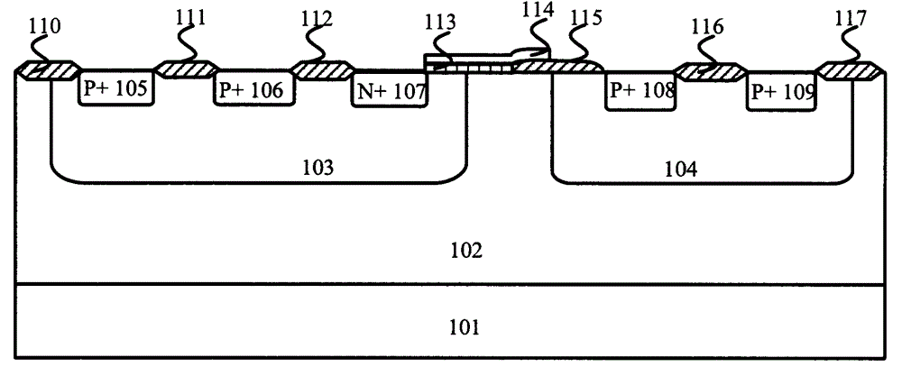
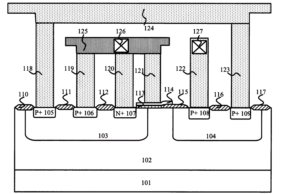
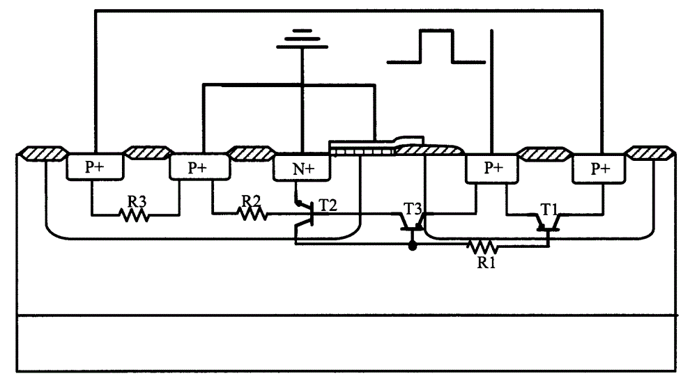
[0004] Aiming at the problems of too low maintenance voltage and insufficient latch-up resistance commonly existing in existing high-voltage ESD protection devices, an example of the present invention designs an ESD protection device with a high maintenance voltage IGBT structure, which not only makes full use of the IGBT device The characteristics of strong current handling ability, and by increasing the layout level of P+ injection and special metal connection, the device can not only form the ESD current discharge path of PNPN structure under the action of high-voltage ESD pulse, but also form a PNP triode and resistor. Another ESD current discharge path connected in series can obtain high sustain voltage, strong robust ESD protection devices suitable for high-voltage IC circuits

Method used


Image

  • ESD protection device of IGBT structure and with high maintaining voltage
  • ESD protection device of IGBT structure and with high maintaining voltage
  • ESD protection device of IGBT structure and with high maintaining voltage

Examples


Embodiment Construction

[0024] Below in conjunction with accompanying drawing and specific embodiment the present invention will be described in further detail:

[0025] An example of the present invention designs an ESD protection device with an IGBT structure with a high sustain voltage, which not only makes full use of the strong current handling capability of the IGBT device, but also enhances the ESD robustness of the device. The increase of the P+ layout structure and the special metal connection can increase the maintenance voltage of the device. By adjusting the key layout size, the device can meet the high-voltage ESD protection in power integrated circuit products with different needs, and no latch-up effect will occur.

[0026] Such as figure 1 The cross-sectional view of the internal structure of the example device of the present invention is shown, specifically an ESD protection device with a high sustain voltage IGBT structure, with a PNPN structure and two ESD current discharge paths i...


PUM


Abstract

An ESD protection device of an IGBT structure and with a high maintaining voltage can be used in an on-chip IC high-voltage ESD protection circuit. The ESD protection device is mainly composed of a P substrate, a high-voltage N well, an N well, a P well, a first P+ injection region, a second P+ injection region, an N+ injection region, a third P+ injection region, a fourth P+ injection region, a metal anode, a metal cathode, a polycrystalline silicon gate, a thin gate oxide layer and a plurality of field oxide isolation regions. According to the ESD protection device of the IGBT structure, under the action of high-voltage ESD pulses, on one hand, a current discharge path with a PNPN structure is formed by the third P+ injection region, the N well, the high-voltage N well, the P well and the N+ injection region, thereby improving failure current of the device and enhancing ESD robustness of the device; and on the other hand, another current discharge path with a parasitic PNP triode and a parasitic resistor being connected in series is formed by the third P+ injection region, the N well, the fourth P+ injection region, the first P+ injection region, the P well and the second P+ injection region, thereby improving the maintaining voltage of the device and enhancing anti-latch capability of the device.

Description

technical field [0001] The invention belongs to the field of electrostatic discharge protection of integrated circuits, relates to a high-voltage ESD protection device, in particular to an ESD protection device with a high sustain voltage IGBT structure, which can be used to improve the reliability of IC high-voltage ESD protection on a chip. Background technique [0002] Electrostatic discharge (ESD) phenomenon is ubiquitous in nature, and it is unavoidable to be affected by ESD in the process of chip production, packaging, testing, storage and transportation. According to the statistics of National Semiconductor Corporation of the United States, ESD phenomenon has become the most important cause of failure of integrated circuit products. one of the reasons. With the rapid development of power semiconductor devices and various advanced high-voltage processes, power integrated circuits have been widely used in people's life and production. At the same time, the performance r...

Claims


Application Information

Patent Timeline
Patent Type & Authority Applications(China)
IPC IPC(8): H01L27/02H01L29/06
Inventor 顾晓峰毕秀文梁海莲黄龙
Owner JIANGNAN UNIV
Learn More