Eureka AIR delivers breakthrough ideas for toughest innovation challenges, trusted by R&D personnel around the world.

Gallium-nitride-based power heterojunction field effect transistor with local back barrier

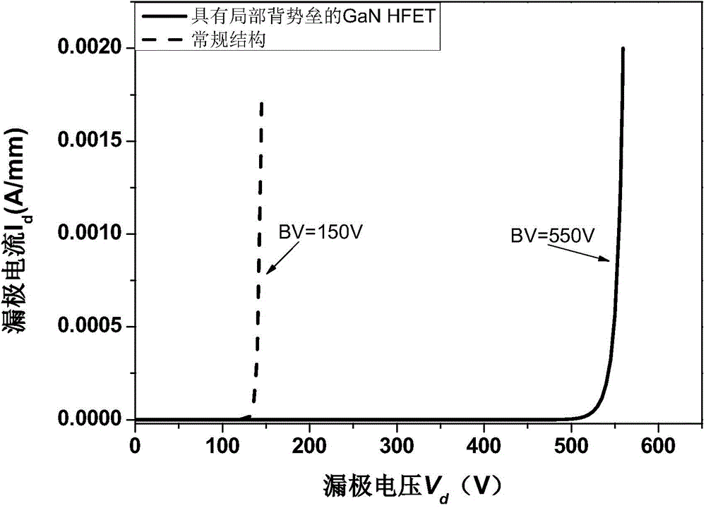
A heterojunction field effect and back barrier technology, applied in semiconductor devices, electrical components, circuits, etc., can solve problems such as increased on-resistance, current collapse effect, and output current drop, to improve withstand voltage, Improve reliability and realize simple effect of device process

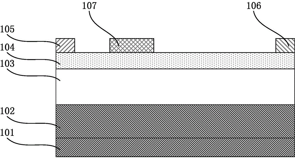
Active Publication Date: 2015-03-11
UNIV OF ELECTRONIC SCI & TECH OF CHINA
View PDF3 Cites 6 Cited by
  • Summary
  • Abstract
  • Description
  • Claims
  • Application Information

AI Technical Summary

Problems solved by technology

However, this technology cannot completely deplete the two-dimensional electron gas in the channel, and cannot give full play to the withstand voltage advantages of GaN materials. At the same time, the deep energy level traps introduced by impurities such as carbon and iron will cause such as increased on-resistance, decreased output current, Negative effects such as current collapse effect and decreased reaction speed

Method used


Image

  • Gallium-nitride-based power heterojunction field effect transistor with local back barrier
  • Gallium-nitride-based power heterojunction field effect transistor with local back barrier
  • Gallium-nitride-based power heterojunction field effect transistor with local back barrier

Examples


Embodiment

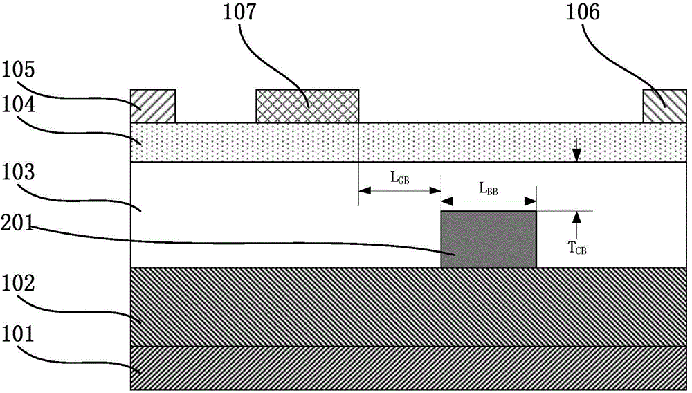
[0026] The GaN HFET structure provided by this embodiment with a local back barrier layer is as follows figure 2 As shown, the main process steps are as follows: sequentially grow an aluminum nitride (AlN) nucleation buffer layer 102 on the substrate by MOCVD, and grow between the gate and drain of the aluminum nitride (AlN) nucleation buffer layer 102 by selective epitaxy Aluminum Indium Gallium Nitride (AlInGaN x In y Ga z N) local back barrier layer 201; then other regions above the nucleation buffer layer 102 start to grow gallium nitride (GaN) channel layer 103, and grow aluminum indium gallium nitride (AlGaN) on the channel layer 103 x In y Ga z N) Barrier layer 104; a source 105 and a drain 106 in ohmic contact with the barrier layer 104 and a gate 107 in Schottky contact are formed on the barrier layer 104.

[0027] The aluminum indium gallium nitride (Al x In y Ga z N) The distance between the local back barrier layer 201 and the drain edge of the gate 107 is...


PUM


Abstract

The invention discloses a gallium-nitride-based power heterojunction field effect transistor with a local back barrier. The gallium-nitride-based power heterojunction field effect transistor is structurally composed of a substrate, an aluminum nitride nucleation buffering layer, an aluminum indium gallium nitride local back barrier layer, a gallium nitride channel layer and an aluminum indium gallium nitride barrier layer mainly from bottom to top, a source electrode, a drain electrode and a grid electrode are formed on the barrier layer, the source electrode and the drain electrode forms ohmic contact with the barrier layer, and the grid electrode forms schottky contact with the barrier layer. By introducing the aluminum indium gallium nitride local barrier layer with polarization intensity larger than the polarization intensity of the gallium nitride channel layer, negative polarization charges are left after interface charges of the aluminum indium gallium nitride barrier layer and the gallium nitride channel layer are balanced, effect of exhausting part of 2DEG of a grid-drain drift region channel is realized, and an LDD (low density drain) structure is formed, so that modulating of electric field distribution of the channel is realized to improve voltage resistance of a device.

Description

technical field [0001] The invention relates to the field of semiconductor devices, in particular to a gallium nitride (GaN)-based power heterojunction field effect transistor with a local back potential barrier. Background technique [0002] Gallium nitride (GaN) based heterojunction field effect transistor has excellent characteristics such as large band gap, high critical breakdown electric field, high electron saturation velocity, good thermal conductivity, radiation resistance and good chemical stability. (GaN) materials can form two-dimensional electron gas heterojunction channels with high concentration and high mobility with materials such as aluminum gallium nitride (AlGaN), so they are especially suitable for applications in high-voltage, high-power and high-temperature environments. One of the transistors with the highest potential for applications. [0003] figure 1 It is a schematic diagram of the existing GaN HFET structure based on GaN-on-Insulator (GOI) tec...

Claims


Application Information

Patent Timeline
IPC IPC(8): H01L29/778H01L29/06
CPCH01L29/0611H01L29/778
Inventor 杜江锋潘沛霖王康刘东于奇
Owner UNIV OF ELECTRONIC SCI & TECH OF CHINA
Why Eureka
Eureka Blog
Learn More