Image pickup element and image pickup device

A technology of imaging elements and pixels, which is applied in electrical components, radiation control devices, electric solid devices, etc., can solve the problems of reducing drift components, reducing sensitivity, controlling acceptor concentration and donor concentration, and achieving dark current suppression, heat dissipation, etc. Effect of Noise Suppression

Active Publication Date: 2015-02-25
SONY SEMICON SOLUTIONS CORP
View PDF9 Cites 4 Cited by
  • Summary
  • Abstract
  • Description
  • Claims
  • Application Information

AI Technical Summary

Problems solved by technology

[0005] However, in a configuration using a chalcopyrite-based compound semiconductor for a photoelectric conversion film employed in a solid-state imaging device as discussed in JP2012-4443A, there is a disadvantage that it is difficult to control the thickness of the depletion layer
This is because, for chalcopyrite-based compound semiconductors, it is difficult to control the acceptor concentration and donor concentration by methods such as ion implantation.
When the photoelectric conversion film is excessively depleted, the depletion layer comes into contact with the interface of the upper electrode, which leads to the generation of dark current
However, when the depletion does not extend to a region where photoelectric conversion occurs, the drift component of charges generated by photoelectric conversion decreases, which lowers the sensitivity

Method used


Image

  • Image pickup element and image pickup device
  • Image pickup element and image pickup device
  • Image pickup element and image pickup device

Examples


example 2

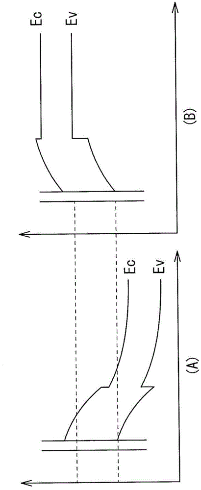
[0067] Figure 6 A cross-sectional structure of an imaging element (imaging element 10B) according to Modification 2 of the above-described embodiment is shown in the figure. In the imaging element 10B, a conductive film 44A and a conductive film 44B spaced apart are formed on the insulating film 13 , and the conductive film 44B formed on the ineffective portion 12B is formed of a light-shielding material. This is a point different from the above-mentioned embodiment. Except for this point, the imaging element 10B has the same configuration as that of the imaging element 10 , and also has the same functions and effects.

[0068] As described above, in the imaging element 10B, the conductive film 44B formed on the invalid portion 12B is formed of a light-shielding material. Therefore, in addition to the effects of the above-described embodiment and Modification 1, there is also an effect that color mixing due to light entering adjacent pixels obliquely can be prevented.

[0...


PUM


Abstract

An image pickup element includes: a photoelectric conversion film provided on a semiconductor substrate and including a chalcopyrite-based compound; an insulating film provided on a light incident surface side of the photoelectric conversion film; and a conductive film provided on the insulating film.

Description

technical field [0001] The present invention relates to an imaging element having a photoelectric conversion portion containing a chalcopyrite compound. The present invention also relates to an imaging device including the imaging element. Background technique [0002] For solid-state imaging devices such as charge coupled device (CCD: charge coupled device) image sensors and complementary metal oxide semiconductor (CMOS: complementary metal oxide semiconductor) image sensors, it is desired to miniaturize the pixel size as the number of pixels increases. At the same time, there is a need to improve moving image performance through high-speed imaging. In such pixel size miniaturization and high-speed imaging, the number of photons entering a unit pixel (solid-state imaging element) decreases, which lowers sensitivity (signal-to-noise ratio (S / N ratio)). Also, for example, a surveillance camera may require a shooting function in dark places. Therefore, it is desired to real...

Claims


Application Information

Patent Timeline
Patent Type & Authority Applications(China)
IPC IPC(8): H01L27/146
CPCH01L31/0322H01L27/14636H01L27/1461H01L27/14621H01L27/14623H01L27/14627H01L27/1464
Inventor 高桥裕嗣
Owner SONY SEMICON SOLUTIONS CORP
Why Eureka
Try Eureka