Through-silicon via structure and method for forming the same

A technology of through-silicon vias and semiconductors, which is applied in the direction of semiconductor/solid-state device parts, semiconductor devices, electrical components, etc., can solve the problems of unstable electrical performance and poor reliability, and achieve improved reliability, stable performance, and avoid accumulation Effect

Active Publication Date: 2018-09-28
CHINA WAFER LEVEL CSP
View PDF4 Cites 0 Cited by
  • Summary
  • Abstract
  • Description
  • Claims
  • Application Information

AI Technical Summary

Problems solved by technology

[0010] However, the existing TSV structure has poor reliability and unstable electrical performance

Method used


Image

  • Through-silicon via structure and method for forming the same
  • Through-silicon via structure and method for forming the same
  • Through-silicon via structure and method for forming the same

Examples


Embodiment Construction

[0034] As mentioned in the background art, the existing TSV structure has poor reliability and unstable electrical performance.

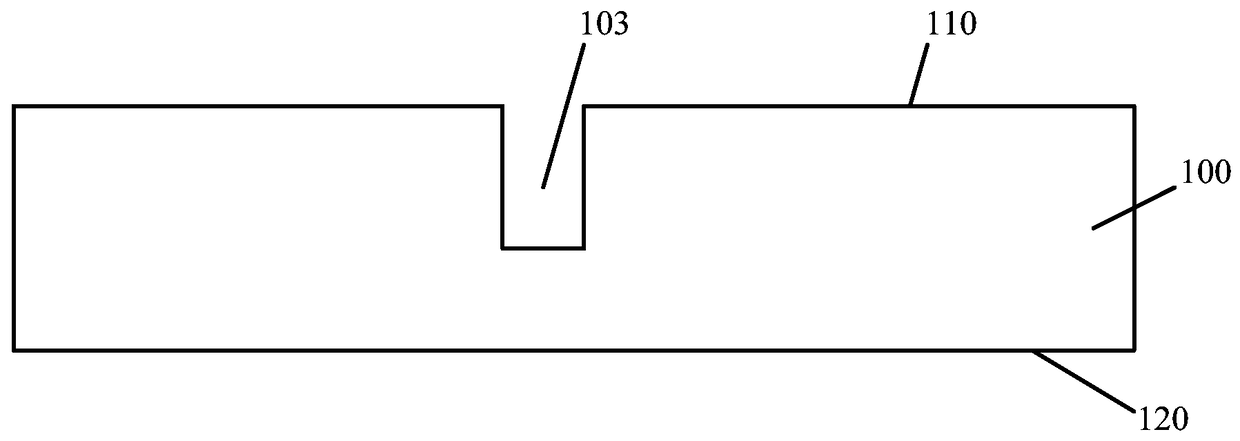
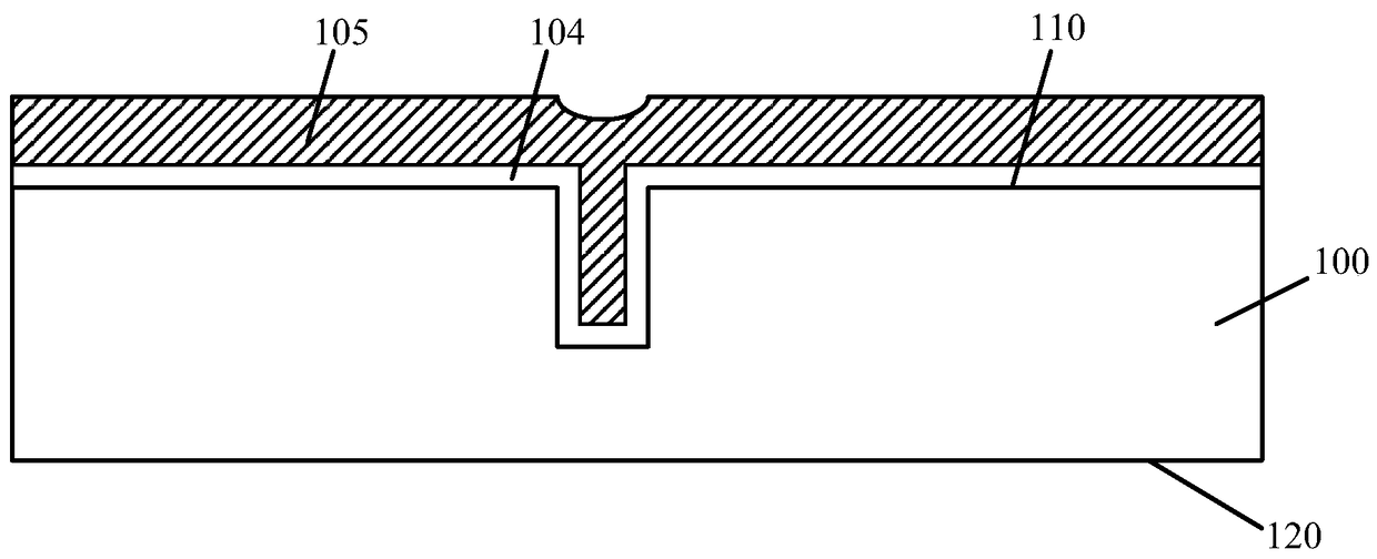
[0035] After research, please continue to refer to figure 2 , the insulating film 104 and the conductive film 105 are formed on the first surface 110 of the substrate 100 and the through hole 103 (please refer to figure 1 ) of the sidewall and bottom surfaces. Since the sidewall of the formed through hole 103 is perpendicular to the first surface 110 of the substrate 100, that is, the sidewall of the through hole 103 and the first surface 110 of the substrate 100 can form a vertex angle at the top of the through hole 103. , and the vertex angle is a right angle, and the stress during the process is easy to accumulate at the vertex 103 of the through hole. The insulating film 104 and the conductive film 105 cover the surface of the corner, therefore, the insulating film 104 on the corner surface at the top of the through hole 103 is easily affect...


PUM


Abstract

The invention discloses a silicon through hole structure and a forming method thereof. The silicon through hole structure comprises a substrate, a through hole formed inside the substrate, a buffer opening formed inside the substrate, a first insulation layer and a conductive layer, wherein the buffer opening is formed in the top of the through hole, the side wall of the buffer opening is inclined relative to the surface of the substrate, the size of the top of the buffer opening is larger than the size of the bottom of the buffer opening, the first insulation layer is located on the surface of the side wall of the buffer opening, the side wall of the through hole and the surface of the bottom of the through hole, and the conductive layer is located on the surface of the first insulation layer. The silicon through hole structure improves the performance and enhances the reliability.

Description

technical field [0001] The invention relates to the technical field of semiconductor manufacturing, in particular to a through-silicon via structure and a forming method thereof. Background technique [0002] With the continuous development of semiconductor manufacturing technology, the feature size of semiconductor devices is continuously reduced, and the integration level of chips is getting higher and higher. However, the current two-dimensional packaging structure has been difficult to meet the growing demand for chip integration, so three-dimensional packaging technology has become a key technology to overcome the bottleneck of chip integration. [0003] The three-dimensional stacking technology based on through silicon vias (Through Silicon Via, TSV) is one of the existing three-dimensional packaging technologies, and the three-dimensional stacking technology based on through silicon vias is one of the main methods to improve chip integration. [0004] The three-dimen...

Claims


Application Information

Patent Timeline
Patent Type & Authority Patents(China)
IPC IPC(8): H01L23/48H01L21/768
CPCH01L2224/11
Inventor 王之奇喻琼杨莹王蔚
Owner CHINA WAFER LEVEL CSP
Why Eureka
Try Eureka