Magnetron sputtering apparatus

A magnetron sputtering device and magnetron sputtering technology, applied in sputtering plating, ion implantation plating, coating, etc., can solve the problems of large-scale processing chambers, which cannot be fully solved, and have not received attention. Achieve the effects of suppressing the increase in replacement frequency, suppressing erosion, and improving production efficiency

Inactive Publication Date: 2015-02-18
TOKYO ELECTRON LTD
View PDF6 Cites 13 Cited by
  • Summary
  • Abstract
  • Description
  • Claims
  • Application Information

AI Technical Summary

Problems solved by technology

However, in the publication, the above-mentioned problem caused by the use of a magnetic target is not paid attention to, and the problem cannot be sufficiently solved.
In addition, in the invention of Japanese Patent Application Laid-Open No. 6-17247, it is necessary to ensure an area for the substrate to move, so there is also a problem of increasing the size of the processing chamber.

Method used


Image

  • Magnetron sputtering apparatus
  • Magnetron sputtering apparatus
  • Magnetron sputtering apparatus

Examples


no. 1 Embodiment approach

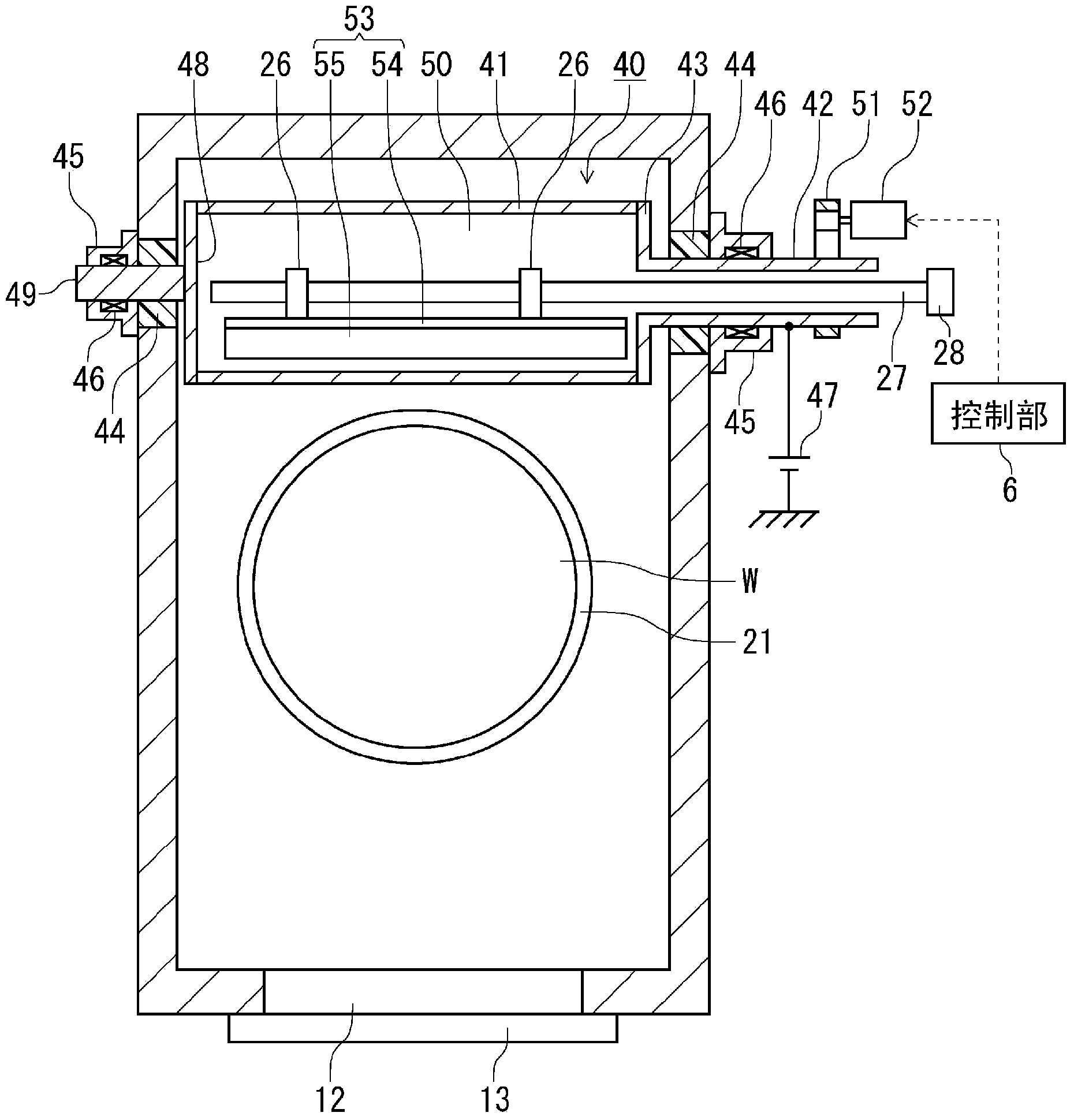
[0057] A magnetron sputtering device 1 according to an embodiment of the present invention will be described with reference to the drawings. figure 1 It is a longitudinal sectional side view of the magnetron sputtering device 1, figure 2 It is a cross-sectional plan view of the magnetron sputtering device 1 . Reference numeral 11 in the figure is a vacuum vessel made of, for example, aluminum (Al) and grounded. Reference numeral 12 in the figure is a transfer port for wafer W serving as a substrate opened on the side wall of vacuum container 11 , and is opened and closed by an opening and closing mechanism 13 .

[0058] A circular table 21 is provided in the vacuum container 11 , and a semiconductor wafer (hereinafter, simply referred to as a wafer) W as a substrate is horizontally placed on the surface of the table 21 . A wafer W having a diameter of, for example, 150 mm to 450 mm can be placed on the stage 21 . The central part of the back surface of the table 21 is con...


PUM

PropertyMeasurementUnit
strengthaaaaaaaaaa

Abstract

[Problem] To provide technology that can increase the productivity of an apparatus when magnetron sputtering is carried out using a target formed from magnetic material. [Solution] The present invention is an apparatus constituted so as to be provided with: a cylindrical body that is a target formed from magnetic material, disposed above a substrate such that the center axis thereof is offset from the center axis of the substrate in a direction along the surface of the substrate; a rotating mechanism that rotates this cylindrical body around the axis of the cylindrical body; a magnet array provided inside a hollow part of the cylindrical body; and a power supply that applies voltage to the cylindrical body. Furthermore, the magnet array has a cross sectional profile, orthogonal to the axis of the cylindrical body, such that the center part protrudes more to the peripheral surface side of the cylindrical body than both end parts in the circumferential direction of the cylindrical body. Thus, even if a target with a comparatively large thickness is used, reductions in the intensity of the magnetic field that leaks from the target can be suppressed, and local progress in erosion can be suppressed.

Description

technical field [0001] The invention relates to a magnetron sputtering device for forming a film on a substrate. Background technique [0002] Magnetic random access memory (MRAM: Magnetic Random Access Memory) and hard disk drives, which are expected to be next-generation memories, use many magnetic materials, and most of these magnetic materials are made of thin films formed on substrates by sputtering of. The MRAM is a memory element in which an insulating film is sandwiched between magnetic films that are ferromagnetic layers, and utilizes a characteristic that the amount of current flow to the insulating film varies depending on whether the magnetization directions of the magnetic films are in the same direction or in opposite directions. [0003] The sputtering is usually carried out using magnetron sputtering, in which the Figure 24 As shown, an apparatus including a circular flat or rectangular flat magnetic target 101 installed in a vacuum container and a pluralit...

Claims


Application Information

Patent Timeline
Patent Type & Authority Applications(China)
IPC IPC(8): C23C14/34C23C14/35
CPCH01J37/3452H01J37/3405H01J37/3455H01J37/3447C23C14/35H01J37/3417C23C14/3407H01J2237/332
Inventor 北田亨中村贯人五味淳宫下哲也
Owner TOKYO ELECTRON LTD
Why Eureka
Try Eureka