Image sensor and method of operation thereof

A technology for image sensors and components, which is applied in the field of complementary metal oxide half-field-effect transistors, and can solve problems such as degradation of color intensity characteristics and reduced sensitivity of image sensors

Inactive Publication Date: 2019-05-07
IUCF HYU (IND UNIV COOP FOUND HANYANG UNIV)
View PDF7 Cites 0 Cited by
  • Summary
  • Abstract
  • Description
  • Claims
  • Application Information

AI Technical Summary

Problems solved by technology

As a result, there will be problems of reduced sensitivity of the image sensor and degradation of color intensity characteristics

Method used


Image

  • Image sensor and method of operation thereof
  • Image sensor and method of operation thereof
  • Image sensor and method of operation thereof

Examples


Embodiment Construction

[0033] Now, specific embodiments according to the present invention will be described in detail with reference to the accompanying drawings. However, the present invention is not limited to these specific embodiments, but can be implemented in various configurations. These specific examples are provided so that the present invention can be fully understood, and the scope of the present invention can be fully understood by those skilled in the art with reference to these specific examples. In the drawings, the same numerals represent the same elements.

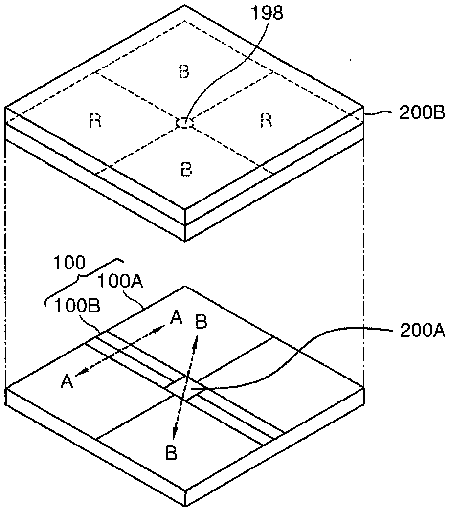
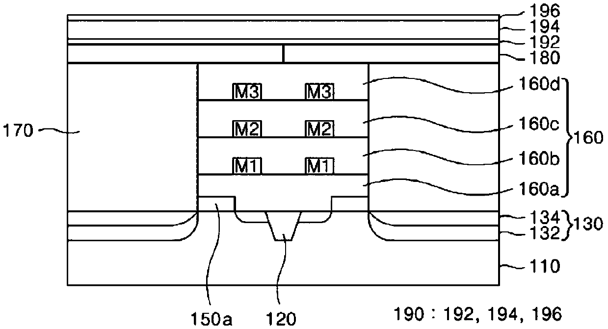
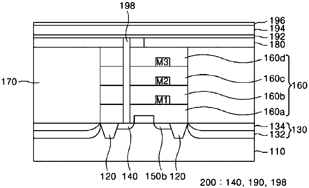
[0034] figure 1 It is a perspective view illustrating an upper portion and a lower portion of an image sensor according to an embodiment of the present invention. figure 2 is taken from along figure 1 The cross-sectional view observed by the A-A line, and image 3is taken from along figure 1 The cross-sectional view observed by the B-B line.

[0035] see figure 1 , an image sensor according to a specific embodiment ...


PUM


Abstract

The invention relates to an image sensor and its operating method. The image sensor includes a first photoelectric conversion component and a second photoelectric conversion component. The first photoelectric conversion part receives various kinds of light other than the light of the first wavelength to generate charges. The second photoelectric conversion part is configured to receive light of the first wavelength to generate charges, wherein at least one of the first photoelectric conversion part and the second photoelectric conversion part is vertically separated from each other.

Description

technical field [0001] The present invention relates to an image sensor and its operating method, and in particular to a Complementary Metal Oxide Silicon (CMOS) image sensor and its operating method. Background technique [0002] Complementary Metal Oxide Semiconductor Field Effect Transistor (CMOS) image sensor includes a plurality of pixels (pixel), each pixel has a photoelectric conversion element (photoelectric conversion element) to convert incident light into an electrical signal, and a metal oxide semiconductor (MOS) transistor The electrical signal can be read from each pixel. The CMOS sensor has the advantages of low voltage and low power consumption, and its application range is wide, so it is extended to be used in a camera in a mobile phone, a digital still camera, a digital video camera, or other similar items. [0003] A CMOS image sensor includes a photodiode, a dielectric layer, a color filter, and a micro lens. A photodiode is formed on the substrate as a...

Claims


Application Information

Patent Timeline
Patent Type & Authority Patents(China)
IPC IPC(8): H01L27/146H04N5/369
CPCH01L27/14621H01L27/14629Y02E10/549H10K39/32H01L27/146H04N25/00H10K30/80
Inventor 朴在勤宋昇弦金志宪金达颢
Owner IUCF HYU (IND UNIV COOP FOUND HANYANG UNIV)
Why Eureka
Try Eureka