
Algorithm and system for dark level correction of cmos image sensor

An image sensor, dark level technology, applied in the electronic field, to achieve the effect of small error, good dark level correction, and good output image

Active Publication Date: 2017-07-07
JILIN FOX PEAK TECH
View PDF5 Cites 0 Cited by
  • Summary
  • Abstract
  • Description
  • Claims
  • Application Information

AI Technical Summary

Problems solved by technology

[0005] The object of the present invention is to provide a kind of algorithm and system thereof for the black level correction of CMOS image sensor, thus solve the aforementioned problems existing in the prior art

Method used


Image

  • Algorithm and system for dark level correction of cmos image sensor
  • Algorithm and system for dark level correction of cmos image sensor
  • Algorithm and system for dark level correction of cmos image sensor

Examples


Embodiment Construction

[0043] In order to make the object, technical solution and advantages of the present invention clearer, the present invention will be further described in detail below in conjunction with the accompanying drawings. It should be understood that the specific embodiments described here are only used to explain the present invention, and are not intended to limit the present invention.

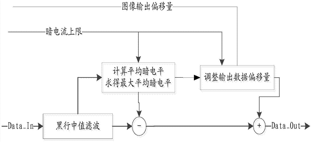
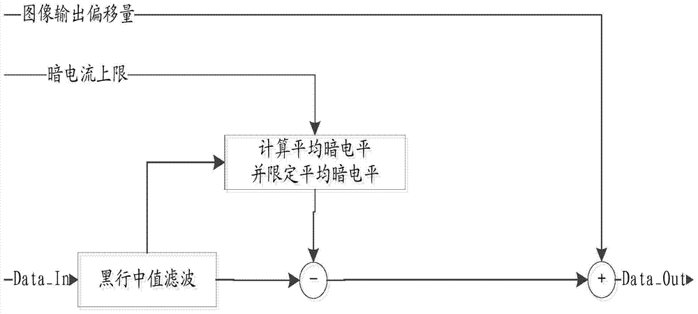
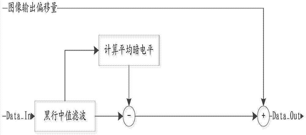
[0044] refer to figure 1 , a kind of algorithm for the dark level correction of CMOS image sensor of the present invention, this algorithm comprises:

[0045] S1. The background system sets the dark level upper limit DC_Lim and the output data offset Offset;

[0046] S2. Inputting an image with dark level information lines;

[0047] S3. Using a median filter algorithm to correct defective pixels in the dark level information row;

[0048] The median filtering described in step S3 can adopt 3-point median filtering, 5-point median filtering or median filtering of more pixels as required; the pix...


PUM


Abstract

The invention discloses an algorithm used for black level correction of a CMOS (Complementary Metal Oxide Semiconductor) image sensor and a system thereof. The algorithm comprises the following steps that S1, a background system configures an upper limit of a black level and an output data offset; S2, the background system inputs an image provided with a black level message line; S3, the background system utilizes a median filtering algorithm to correct a defect pixel of the black level message line; S4, the background system computes an average black level of each pixel channel of the black level message line after filtering correction; S5, the background system adjusts the output data offset; S6, the background system carries out black level correction on the input image data; and S7, the background system outputs a normal image. The system comprises a defect pixel correction module, a correction information computation module and a black level correction module, wherein the correction information computation module comprises an average black level computation module and a data output offset regulation module. According to the algorithm used for black level correction of the CMOS image sensor and the system thereof, the black level correction can be better carried out, the error is small, and the problems of color deviation and brightness unsaturation under the condition of a larger black level difference of four color channels are solved.

Description

technical field [0001] The invention relates to the field of electronic technology, in particular to an algorithm and system for black level correction of a CMOS image sensor. Background technique [0002] In recent years, due to the advantages of low cost, low voltage, and low power consumption, CMOS image sensors integrating photosensitive devices, analog readout circuits, digital control systems, and intelligent signal processing circuits have become more and more attractive. However, the dark current severely limits the performance of the CMOS image sensor, such as dynamic range and sensitivity, and causes FPN (fixed pattern noise, fixed pattern noise) and transient noise, thereby also reducing its noise performance. Since the dark current mainly comes from the interface defects in the field oxygen region and the boundary of the money slot isolation, it is more and more challenging to manufacture an image sensor with a low dark level as CMOS technology enters the deep su...

Claims


Application Information

Patent Timeline
Patent Type & Authority Patents(China)
IPC IPC(8): H04N5/361
Inventor 谷元保姚洪涛
Owner JILIN FOX PEAK TECH
Learn More