
Flip Chip Semiconductor Package Structure

A packaging structure, flip-chip technology, applied in the direction of semiconductor devices, semiconductor/solid-state device components, electric solid-state devices, etc., can solve the problems of failure of semiconductor devices, weak coupling, poor contact between semiconductor chips and lead frames, etc. Reliable electrical connection, increased mechanical strength, and the effect of preventing solder from flowing away from the interconnection

Active Publication Date: 2017-09-29
NANTONG FUJITSU MICROELECTRONICS
View PDF3 Cites 0 Cited by
  • Summary
  • Abstract
  • Description
  • Claims
  • Application Information

AI Technical Summary

Problems solved by technology

[0004] Due to the defects of the forming method, it will inevitably cause a series of defects in the package structure itself, such as poor contact between the semiconductor chip and the lead frame, weak coupling, etc.
These will lead to the failure of semiconductor devices

Method used


Image

  • Flip Chip Semiconductor Package Structure
  • Flip Chip Semiconductor Package Structure
  • Flip Chip Semiconductor Package Structure

Examples


Embodiment Construction

[0029] In order to make the above objectives, features, and advantages of the present invention more obvious and understandable, the specific embodiments of the present invention will be further described in detail below in conjunction with the accompanying drawings.

[0030] In the following description, specific details are set forth in order to fully understand the present invention. However, the present invention can be implemented in many other ways different from those described herein, and those skilled in the art can make similar extensions without departing from the connotation of the present invention. Therefore, the present invention is not limited by the specific implementation disclosed below.

[0031] In view of the above defects, the present invention provides a flip-chip semiconductor package structure.

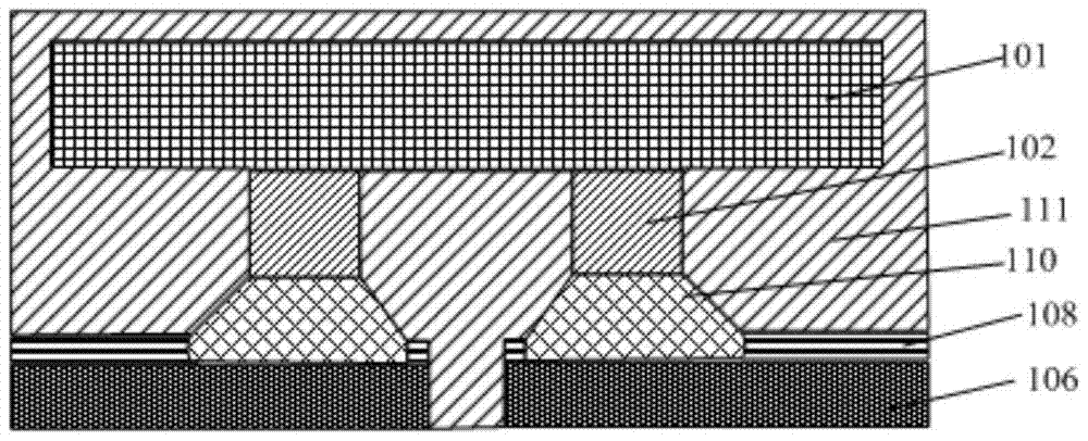
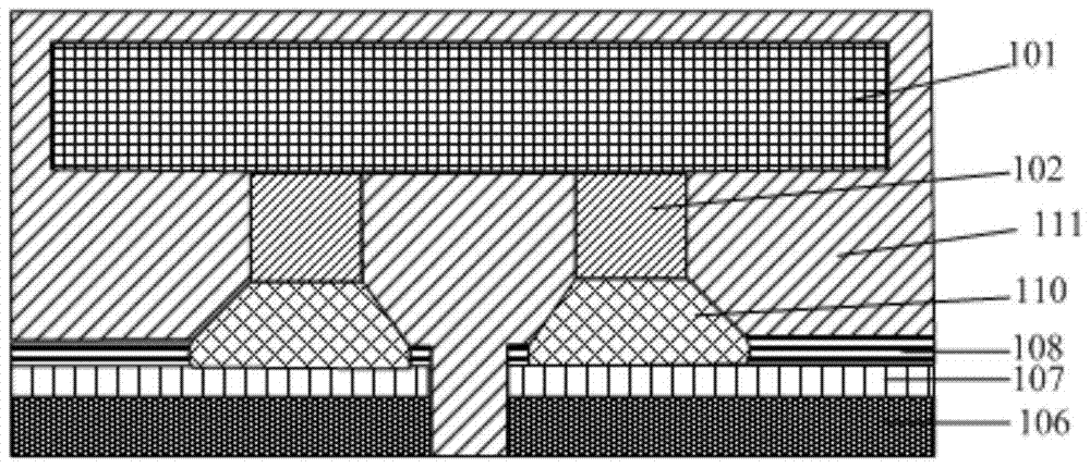
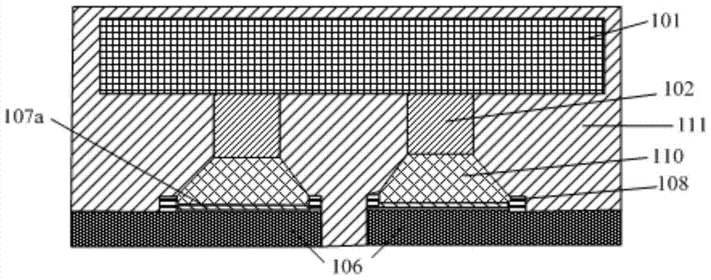
[0032] reference figure 1 , The first embodiment of the present invention provides a flip-chip semiconductor package structure, including:

[0033] A semiconductor c...


PUM


Abstract

The invention discloses a flip-chip semiconductor packaging structure. Includes: semiconductor chip, multiple copper pillars, lead frame, insulating layer on the surface of the lead frame, multiple solder interconnects, and molding compound. The surface of the semiconductor chip has pad patterns on which the copper pillars are formed. The insulating layer has an opening, the area of ​​the opening is larger than the cross-sectional area of ​​the copper column, and the opening exposes part of the leads on the lead frame. The solder interconnection is located between the copper pillar and the portion of the lead exposed by the opening, and the molding compound is used to encapsulate the assembly. The flip chip semiconductor package structure enables a semiconductor chip to be firmly coupled to a lead frame while preventing poor contact therebetween.

Description

Technical field [0001] The present invention relates to the field of semiconductor technology, in particular to a flip chip semiconductor packaging structure. Background technique [0002] As time goes by, semiconductor packaging structures are becoming smaller and more concentrated, and are manufactured into various shapes. According to the connection method, the semiconductor package structure is typically classified into a wire bonding type or a flip chip bonding type. The wire bonding type packaging structure uses conductive bonding wires to connect the electrodes of the semiconductor chip to the lead frame, while the flip chip type packaging structure uses conductive bumps placed on the electrode pads of the semiconductor chip. To connect the semiconductor to the lead or directly connect the semiconductor chip to the connection terminal of the circuit board. Flip-chip bonding type package structure has a shorter electrical connection path than metal bonding type package st...

Claims


Application Information

Patent Timeline
Patent Type & Authority Patents(China)
IPC IPC(8): H01L23/31H01L23/495
CPCH01L2224/16245
Inventor 石磊
Owner NANTONG FUJITSU MICROELECTRONICS
Learn More