
Laser-chemical preparation method of monocrystal silicon substrate sub-micron pyramid structure

A technology of pyramid structure and single crystal silicon, which is applied in chemical instruments and methods, single crystal growth, single crystal growth, etc., can solve the problems of high environmental requirements, achieve high controllability, simple process, ensure periodicity and uniformity effect

Active Publication Date: 2014-12-10
BEIJING UNIV OF TECH
View PDF4 Cites 8 Cited by
  • Summary
  • Abstract
  • Description
  • Claims
  • Application Information

AI Technical Summary

Problems solved by technology

Although nanoimprinting can obtain higher graphics resolution, the thermal embossing method needs to be prepared under high temperature and high pressure, which has high requirements on the environment, and because its graphic accuracy is closely related to the precision of the mold, the resolution of the mold There are high requirements on rate, planarization, uniformity, surface energy, etc.

Method used


Image

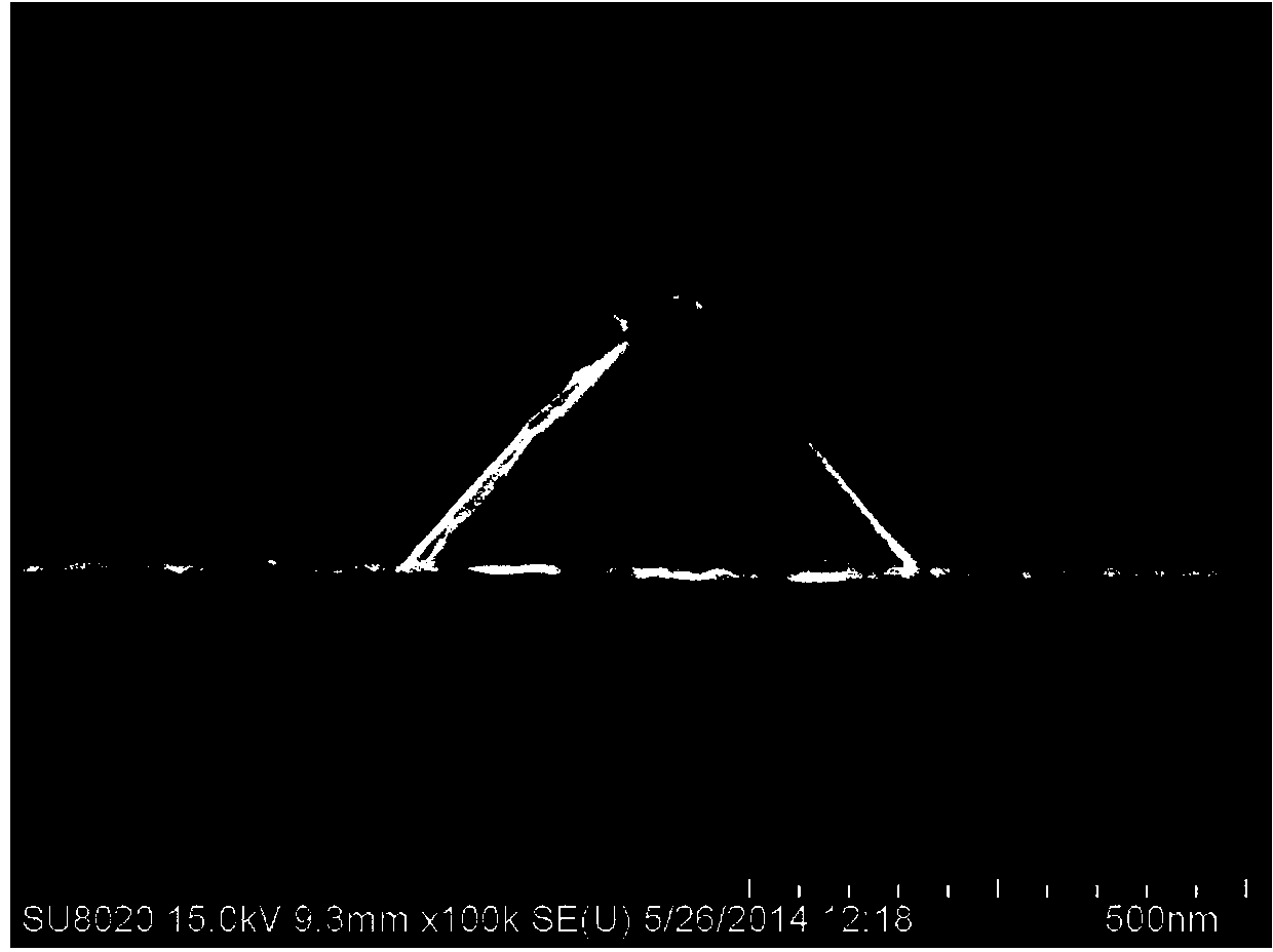
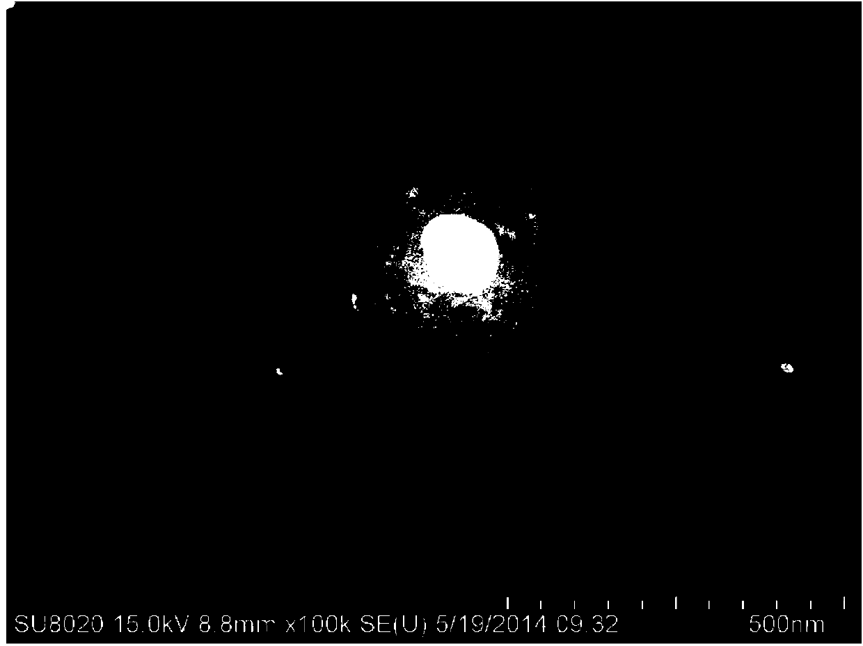
  • Laser-chemical preparation method of monocrystal silicon substrate sub-micron pyramid structure
  • Laser-chemical preparation method of monocrystal silicon substrate sub-micron pyramid structure
  • Laser-chemical preparation method of monocrystal silicon substrate sub-micron pyramid structure

Examples


Embodiment 1

[0023] Soak the monocrystalline silicon in acetone solution for 6 minutes; soak in HF solution with a mass fraction of 10% for 10 minutes; immerse in ethanol solution for 6 minutes, rinse and dry; A single layer of SiO with hexagonal close-packed distribution is arranged on the surface of the sheet sample 2 Place the microspheres in the air to dry naturally for 1 hour; place the monocrystalline silicon sample on the target platform, adjust the optical path so that the uniform beam spot size is larger than the sample size, and perform single-pulse irradiation. The laser is an excimer laser with a wavelength of 248nm ; Using pulse energy density 150mJ / cm 2 , with a frequency of 3 Hz; immerse the irradiated monocrystalline silicon sample in ethanol solution for 5 minutes; soak in 10% HF solution for 10 minutes to remove residual SiO 2 Microspheres: Immerse the cleaned monocrystalline silicon sample in an aqueous sodium hydroxide solution containing ethanol, corrode it for 30 sec...

Embodiment 2

[0026] Soak the monocrystalline silicon in acetone solution for 10 minutes; immerse in HF solution with a mass fraction of 15% for 6 minutes; immerse in ethanol solution for 10 minutes, rinse and dry; A single layer of SiO with hexagonal close-packed distribution is arranged on the surface of the sheet sample 2 Place the microspheres in the air to dry naturally for 1 hour; place the monocrystalline silicon sample on the target platform, adjust the optical path so that the uniform beam spot size is larger than the sample size, and perform single-pulse irradiation. The laser is an excimer laser with a wavelength of 248nm ; Using pulse energy density 400mJ / cm 2 , with a frequency of 3 Hz; immerse the irradiated monocrystalline silicon sample in ethanol solution for 5 minutes; soak in HF solution with a mass fraction of 15% for 10 minutes to remove residual SiO 2 Microspheres; immerse the cleaned monocrystalline silicon sample in an aqueous sodium hydroxide solution containing et...

Embodiment 3

[0029] Soak the monocrystalline silicon in acetone solution for 8 minutes; immerse in 5% HF solution for 8 minutes; immerse in ethanol solution and ultrasonically clean it for 8 minutes, rinse and dry; A single layer of SiO with hexagonal close-packed distribution is arranged on the surface of the sheet sample 2 Place the microspheres in the air to dry naturally for 1 hour; place the monocrystalline silicon sample on the target platform, adjust the optical path so that the uniform beam spot size is larger than the sample size, and perform single-pulse irradiation. The laser is an excimer laser with a wavelength of 248nm ; Using pulse energy density 100mJ / cm 2 , with a frequency of 3 Hz; immerse the irradiated monocrystalline silicon sample in ethanol solution for 5 minutes; immerse in HF solution with a mass fraction of 15% for 8 minutes to remove residual SiO 2Microspheres: Immerse the cleaned monocrystalline silicon sample in an aqueous solution of sodium hydroxide containi...


PUM


Abstract

The invention discloses a laser-chemical preparation method of a monocrystal silicon substrate sub-micron pyramid structure, belonging to the field of crystalline silicon surface micro-structure preparation. The preparation method comprises the following steps: firstly, performing pretreatment on monocrystal silicon, and covering periodically close-packed microspheres on the surface of monocrystal silicon; performing irradiation by adopting a 248nm laser, wherein the single pulse energy density is 100-400mJ / cm<2>; performing certain treatment on a monocrystal silicon sample after irradiation, and removing the residual microspheres on the surface; after removal ends, dipping the monocrystal silicon sample into a sodium hydroxide aqueous solution containing ethanol under the environment that the water bath temperature is 70-80 DEG C, eroding for 10-30 seconds, taking out the monocrystal silicon sample, and washing by using deionized water to obtain a monocrystal silicon piece with a normal pyramid array. The laser-chemical preparation method disclosed by the invention exerts the laser controllability, can be used for rapidly and simply preparing the pyramid array with periodicity and uniformity, has high controllability in pyramid forming, can be used for adjusting the separation distance and morphology features of the pyramid array, also is low in raw material cost, and has relatively high practicability.

Description

technical field [0001] The invention belongs to the field of crystal silicon surface microstructure preparation. Background technique [0002] Effectively adjusting the surface microstructure of single crystal silicon is a focus in the field of semiconductor research. Periodically ordered pyramid arrays not only have special size and shape effects, but also have good optical, electrical, and magnetic properties. The conventional method of preparing pyramids is to use the anisotropic corrosion properties of alkaline solution to single crystal silicon, and to control the size and shape characteristics of the pyramids by adjusting the concentration of alkaline solution and the concentration of additives. The prepared pyramids are completely devoid of periodicity and uniformity. Moreover, in order to obtain a pyramid structure with a large coverage area, a certain period of alkaline etching is required. Feng Shimeng's group at Shanghai Jiao Tong University can control the etchi...

Claims


Application Information

Patent Timeline
Patent Type & Authority Applications(China)
IPC IPC(8): C30B33/10C30B33/04C30B29/06
Inventor 季凌飞林真源吴燕吕晓占闫胤洲蒋毅坚
Owner BEIJING UNIV OF TECH
Learn More