Method and device for firmly welding SMD (surface mounted devices) nuts on printed circuit boards

A technology of printed circuit boards and nuts, which is applied in the direction of assembling printed circuits with electrical components, can solve problems such as failure to meet the requirements of product reliability testing, and achieve the effects of long service life, firm connection, and prevention of falling off

Active Publication Date: 2014-10-29
TAICANG T&W ELECTRONICS CO LTD
View PDF5 Cites 3 Cited by
  • Summary
  • Abstract
  • Description
  • Claims
  • Application Information

AI Technical Summary

Problems solved by technology

However, the reliability of SMT nuts has been strongly watched, and the traditional packaging and manufacturing methods of SMD nuts cannot meet the requirements of product reliability testing.

Method used


Image

  • Method and device for firmly welding SMD (surface mounted devices) nuts on printed circuit boards
  • Method and device for firmly welding SMD (surface mounted devices) nuts on printed circuit boards
  • Method and device for firmly welding SMD (surface mounted devices) nuts on printed circuit boards

Examples


Embodiment 1

[0017] A method for firmly welding SMD nuts on a printed circuit board. The first step is to cut the nut steel mesh. The area of ​​the nut steel mesh is larger than the contact surface between the nut and the PCB board. The second step is to open holes on the nut steel mesh and open the nut legs. Pillar hole, the radius of the hole is smaller than the radius of the post hole on the PCB. The third step is to install the nut steel mesh, brush the solder paste, and then paste the SMD nut on the pad coated with solder paste. Because the nut steel mesh The radius is smaller than the opening radius of the pin hole on the PCB. When the nut is attached to the pad coated with solder paste, a little solder paste will be attached to the pin), the fourth step is through reflow soldering, in the environment of high temperature 220-250 , Let the solder paste melt, and the excess solder paste flows along the hole of the column foot. After the alloy composition is cooled and solidified, solder...

Embodiment 2

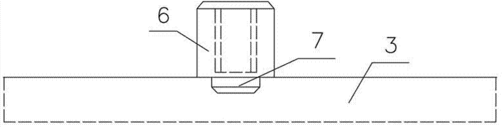
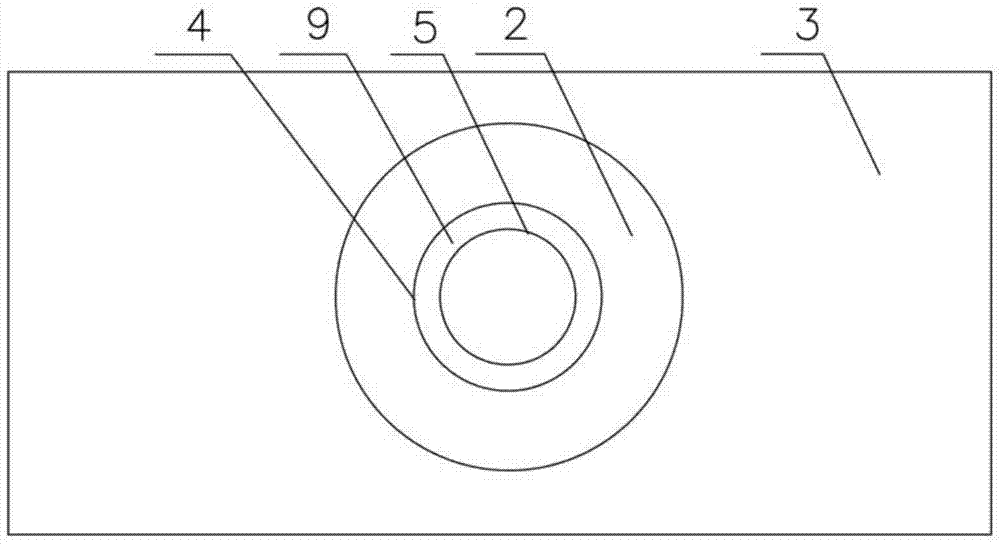
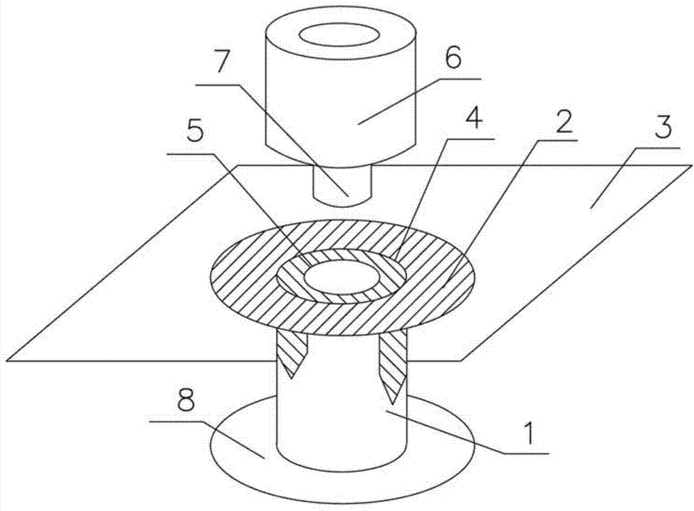
[0019] A device for firmly welding SMD nuts on a printed circuit board, comprising: a nut leg, the nut leg is connected to a nut steel mesh 2, and both the nut leg and the nut steel mesh are connected to a PCB Board 3, the nut stencil opening 5, the nut foot column opening column foot hole 4, the insertion column 7 of the nut 6 is inserted into the column foot hole, and the nut is connected through the hole on the PCB to the BOT side of the PCB.

[0020] attached image 3 The entire shadow plane is the nut steel mesh. After being heated, the solder paste flows through the hole 5 and flows into the inner wall of the pcb column foot hole 4. image 3 Part number 1 is a three-dimensional view of the PCB opening, which is the through hole used when the pin is inserted into the PCB.

Embodiment 3

[0022] The device for firmly welding the SMD nut described in embodiment 2 on a printed circuit board, the outer diameter of the nut is 3.15-3.25mm, the height is 3.00-3.05mm, and the diameter of the post is 1.97-2.00mm , the height is 0.60-0.65mm.


PUM


Abstract

The invention discloses a method and a device for firmly mounting SMD (surface mounted devices) nuts on printed circuit boards. Further reduction of costs is a key of success or failure if the profit margin is required to be increased in the electronic industry at present. The method for firmly welding the SMD nuts on the printed circuit boards includes firstly, tailoring nut steel meshes with the areas larger than the contact areas of the nuts and the PCBs (printed circuit boards); secondly, perforating holes in the nut steel meshes and perforating leg holes in legs of the nuts; thirdly, fitting the legs of the nuts with the PCBs, arranging the nut steel meshes between the legs of the nuts and the PCBs; fifthly, filling solder paste along contact positions of the legs of the nuts and the PCBs, inserting the legs of the nuts into the leg holes when the solder paste flows to the inner walls of the leg holes along the insides of the leg holes, and completely welding the nuts on the printed circuit boards when the nuts, the PCBs and the leg holes are firmly adhered with one another. The radius of each hole is larger than that of each leg hole. The method and the device are applicable to SMD nut elements.

Description

Technical field: [0001] The invention relates to a method and a device for firmly welding an SMD nut on a printed circuit board. Background technique: [0002] At present, in order to increase profit margins in the electronics industry, further cost reduction is the key to success or failure. This requires electronic products to be more and more "light, thin, short, small" and multi-functional. Low-cost PCB (Printed circuit board, printed circuit board) and manufacturing are urgently required. [0003] Double-sided mount-SMT (Surface Mount Technology, surface mount technology) is better than double-sided mount-insert mixed-SMT&DIP (dual inline-pin package, in-line packaging technology) process form, which simplifies the operation process and improves processing efficiency , reducing the cost of manpower, time and materials. [0004] SMD (Surface Mounted Devices, Surface Mount Devices) nuts replace traditional DIP nuts in due course. However, the reliability of SMT nuts h...

Claims


Application Information

Patent Timeline
Patent Type & Authority Applications(China)
IPC IPC(8): H05K3/34
Inventor 张丽周燚俊
Owner TAICANG T&W ELECTRONICS CO LTD
Why Eureka
Try Eureka