Compensation circuit applied to liquid crystal display panel and display device
A liquid crystal display panel and compensation circuit technology, applied to static indicators, instruments, etc., can solve problems such as over-brightness or over-darkness, screen flickering, over-deflection, etc., to prevent charge polarization, suppress screen flickering, and avoid abnormal The effect of symmetrical deflection
- Summary
- Abstract
- Description
- Claims
- Application Information
AI Technical Summary
Problems solved by technology
Method used
Image
Examples
Embodiment 1
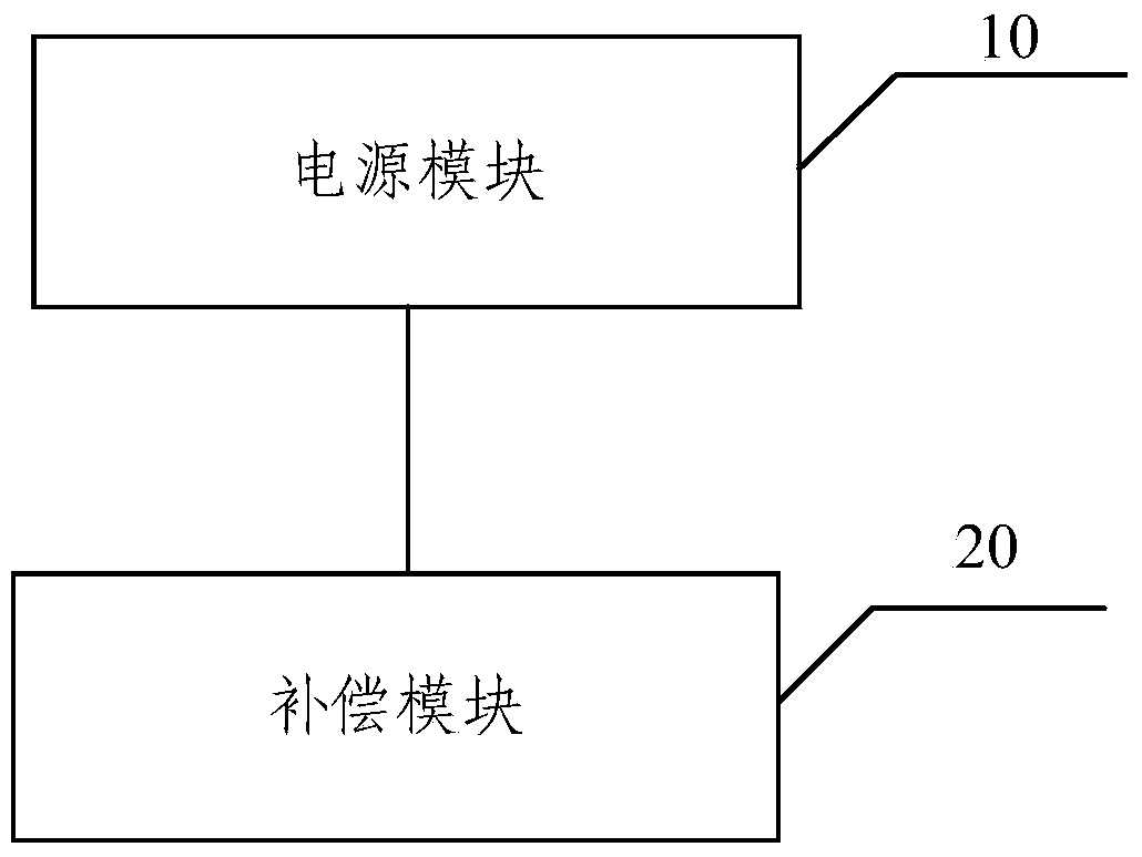
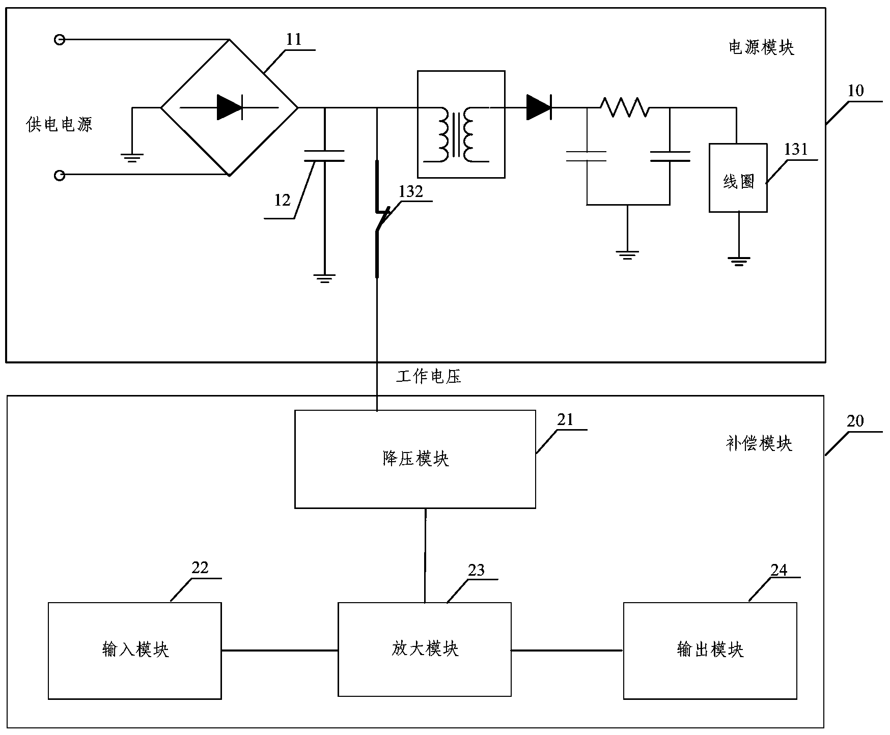
[0031] This embodiment provides a compensation circuit applied to a liquid crystal display panel, including a power supply module 10 and a compensation module 20. The specific circuit schematic diagram is as follows figure 2 shown. The power supply module 10 includes a rectifier 11, a capacitor 12 and a relay. The input end of the rectifier 11 is connected to the power supply, the output end of the rectifier 11 is connected to the first end of the capacitor 12 and the first end of the relay, and the second end of the capacitor 12 is grounded. The rectifier 11 is used to convert the power supply from alternating current to direct current, the capacitor 12 is used to store and release charges, and the relay controls its contacts to provide working voltage to the compensation circuit 20 according to whether the power supply is turned on.
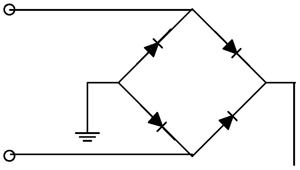
[0032] Optionally, the rectifier 11 is a full-bridge rectifier, which connects the alternating current to the full-bridge rectifier. The full...
Embodiment 2
[0039] This embodiment also provides a compensation circuit applied to a liquid crystal display panel, and its specific circuit schematic diagram is as follows image 3 As shown, the power supply module 10 also includes a rectifier 11, a capacitor 12 and a relay, and the circuit structure and working principle are the same as those in the first embodiment, and are not repeated here.
[0040] The difference from the first embodiment is that the compensation module 20 in this embodiment includes a Zener diode 25, a filter capacitor 26 and a transistor 27, wherein the Zener diode 25 and the filter capacitor 26 are connected in parallel, and the Zener diode 25 and the filter capacitor 26 are connected in parallel. One end is connected to the output end of the power module 10 and the gate of the transistor 27, the other end of the Zener diode 25 and the filter capacitor 26 is grounded, the first end of the transistor 27 is grounded, and the second end outputs the compensated common ...
Embodiment 3
[0045] In order to solve the above technical problems, the present invention also provides a display device, which not only includes a display panel 30 on which common electrode lines are arranged, but also includes the compensation applied to the liquid crystal display panel in Embodiment 1 or Embodiment 2. circuit, the schematic diagrams of the display device are as follows Figure 5 , Image 6 As shown, the compensation module applied to the liquid crystal display panel provides a compensated common voltage to the common electrode lines on the display panel 30 .
[0046] Since the input module 22, the amplifying module 23 and the output module 24 can form a loop with the display panel 30, the common voltage can be compensated, that is, the input module 22 receives the common voltage fed back by the display panel 30 and transmits it to the amplifying module 23 (ie, Amplifier) for amplification, and then sent back to the display panel 30 by the output module 24 . If there...
PUM
 Abstract
Description
Claims
Application Information
 - R&D
- Intellectual Property
- Life Sciences
- Materials
- Tech Scout
- Unparalleled Data Quality
- Higher Quality Content
- 60% Fewer Hallucinations
Browse by: Latest US Patents, China's latest patents, Technical Efficacy Thesaurus, Application Domain, Technology Topic, Popular Technical Reports.
© 2025 PatSnap. All rights reserved.Legal|Privacy policy|Modern Slavery Act Transparency Statement|Sitemap|About US| Contact US: help@patsnap.com


