
Non-disk cavity semiconductor laser with wavelength choice grating

A wavelength selection, semiconductor technology, applied in the field of microcavity lasers, can solve the problems of information distortion, low detection efficiency, logic errors, etc., and achieve the effect of high side mode suppression ratio and narrow spectral line width

Active Publication Date: 2014-10-15
CHANGCHUN UNIV OF SCI & TECH
View PDF5 Cites 5 Cited by
  • Summary
  • Abstract
  • Description
  • Claims
  • Application Information

AI Technical Summary

Problems solved by technology

The multi-wavelength lasing characteristics prevent the device from being used in fields that require a single wavelength, such as optical information communication, optical information logic calculation, optical information detection, etc. Otherwise, information distortion, logic errors, and low detection efficiency will occur.

Method used


Image

  • Non-disk cavity semiconductor laser with wavelength choice grating
  • Non-disk cavity semiconductor laser with wavelength choice grating
  • Non-disk cavity semiconductor laser with wavelength choice grating

Examples


Embodiment Construction

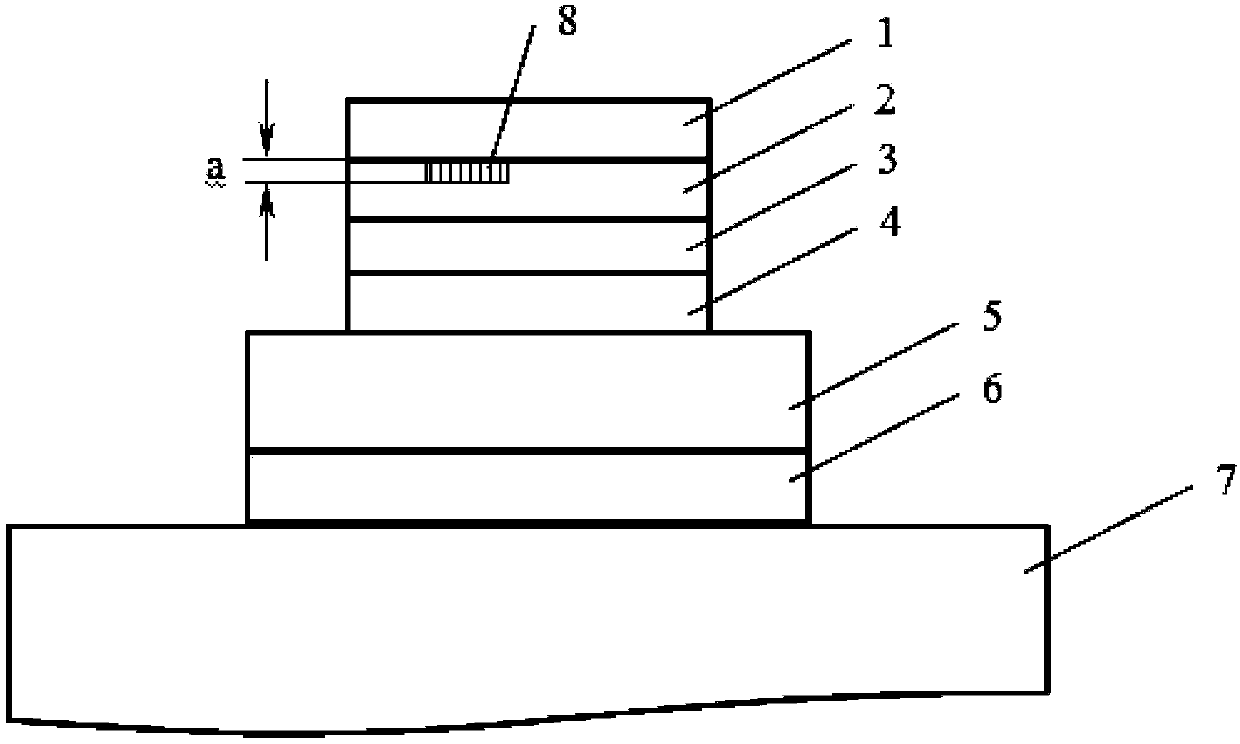
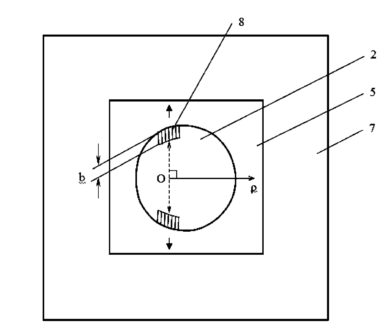
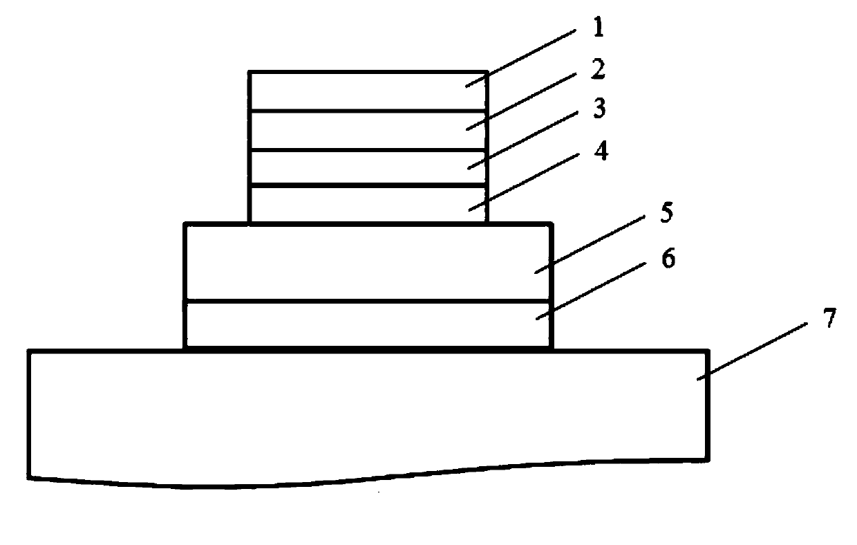
[0011] Such as figure 2 , image 3 As shown, the non-disc cavity semiconductor laser with wavelength selection grating of the present invention is an upper electrode 1, an upper waveguide layer 2, an active gain region 3, a lower waveguide layer 4, a substrate 5, and a lower electrode from top to bottom. 6. Heat sink 7. Both the upper electrode 1 and the lower electrode 6 are gold electrodes. Both the upper waveguide layer 2 and the lower waveguide layer are InGaAsP layers. The active gain region 3 is an InGaAs / InAlAs quantum well cascaded structure. The material of the substrate 5 is InP. The heat sink 7 is a copper plate. The lower electrode 6 is directly welded on the heat sink 7 by solder. Alternatively, an AlN (aluminum nitride) heat sink is welded between the lower electrode 6 and the heat sink 7 . The upper waveguide layer 2, the active gain region 3, and the lower waveguide layer 4 have outer boundaries of the same shape, and the outer boundary curve is type ...


PUM


Abstract

The invention discloses a non-disk cavity semiconductor laser with a wavelength choice grating, and belongs to the technical field of microcavity lasers. The lasing spectrum of the existing structural microcavity laser has the characteristic of multi-wavelength lasing, so that the laser cannot be used in the field requiring single wavelength work. In the non-disk cavity semiconductor laser, an upper waveguide layer, an active gain region and a lower waveguide layer are provided with outer boundaries with the same shape; a curve of the outer boundaries is a Limacon curve; a polar equation of the Limacon curve is as shown in the specification, wherein R(phi) is the polar radius, phi is a polar angle, R0 is the characteristic radius, and epsilon is a deformation factor and is equal to 0.35-0.45; a starting point of the Limacon curve is 0 degree; and two oriented optical coupling output positions are 90 degrees and 270 degrees respectively. The non-disk cavity semiconductor laser is characterized in that the wavelength choice grating is arranged on the edge of the upper waveguide layer corresponding to 90 degrees or / and 270 degrees of the outer boundaries. The scheme can obtain single wavelength light output.

Description

technical field [0001] The invention relates to a non-disk cavity semiconductor laser with a wavelength selection grating, belonging to the technical field of micro cavity lasers. Background technique [0002] Among microcavity lasers, compared with disk cavity semiconductor lasers, non-disc cavity semiconductor lasers have the characteristics of directional optical coupling output. This kind of microcavity laser is suitable for laser communication, laser detection, basic research, medical treatment, etc. Typical non-disk cavity semiconductor lasers are Type structure microcavity laser, the scheme was published in "Applied Physics Letters" No. 94, page 251101, published in June 2009. said The structural characteristics of the type structure microcavity laser are as follows. like figure 1 As shown, from top to bottom are upper electrode 1 , upper waveguide layer 2 , active gain region 3 , lower waveguide layer 4 , substrate 5 , lower electrode 6 , and heat sink 7 . The...

Claims


Application Information

Patent Timeline
Patent Type & Authority Applications(China)
IPC IPC(8): H01S5/14
Inventor 晏长岭史建伟冯源郝永芹李鹏
Owner CHANGCHUN UNIV OF SCI & TECH
Learn More