High polarization ratio single photon detector based on superconductive nanowires
A single-photon detector and superconducting nanowire technology, applied in the field of light detection, can solve the problems of low polarization ratio, large volume, and complex structure of polarization detection devices, and achieve the effects of low dark count, small volume, and simple structure
- Summary
- Abstract
- Description
- Claims
- Application Information
AI Technical Summary
Problems solved by technology
Method used
Image
Examples
Embodiment 1
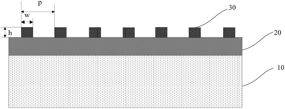
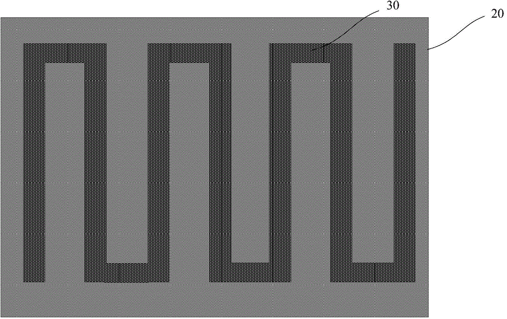
[0042] Such as Figure 1 ~ Figure 2 and Figure 4 As shown, this embodiment provides a high polarization ratio single photon detector based on superconducting nanowires, which includes:
[0043] Substrate 10;
[0044] An anti-reflection layer 20, bonded to the surface of the substrate 10;
[0045] Superconducting nanowires 30 are bonded to the surface of the anti-reflection layer 20 in a periodic meandering structure, the width of the superconducting nanowires 30 is not greater than 75 nanometers, the thickness is not less than 7 nanometers, and the duty cycle is not greater than 40%.
[0046] As an example, the superconducting nanowire-based high polarization ratio single-photon detector of this embodiment is a superconducting nanowire 30 single-photon detector with a front-incidence structure.
[0047] As an example, the polarization ratio of the single photon detector decreases as the width of the superconducting nanowire 30 increases, and increases as the thickness inc...
Embodiment 2
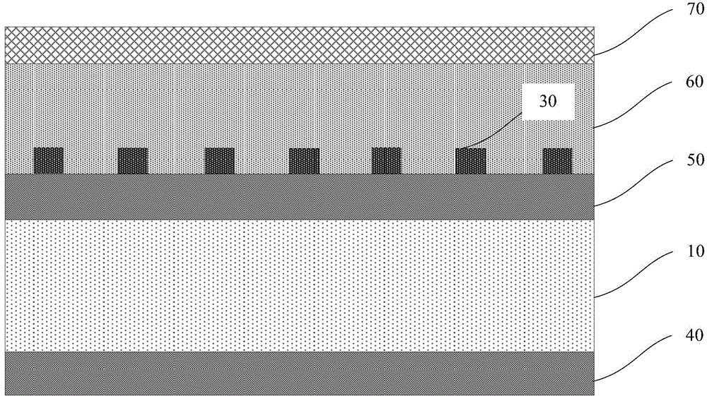
[0056] Such as image 3 As shown, this embodiment also provides a high polarization ratio single photon detector based on superconducting nanowires, including:
[0057] A substrate 10, the upper and lower surfaces of the substrate 10 are respectively combined with an upper anti-reflection layer 50 and a lower anti-reflection layer 40;
[0058] The optical cavity structure 60 is combined with the surface of the upper anti-reflection layer 50;
[0059] A mirror 70, combined with the surface of the optical cavity structure 60;
[0060] The superconducting nanowire 30 is combined in a periodic meandering structure between the upper anti-reflection layer 50 and the optical cavity structure 60, the width of the superconducting nanowire 30 is not greater than 75 nanometers, and the thickness is not less than 7 nanometers, the duty cycle is no greater than 40%.
[0061] As an example, the superconducting nanowire-based high polarization ratio single-photon detector of this embodime...
PUM
 Abstract
Description
Claims
Application Information
 - R&D
- Intellectual Property
- Life Sciences
- Materials
- Tech Scout
- Unparalleled Data Quality
- Higher Quality Content
- 60% Fewer Hallucinations
Browse by: Latest US Patents, China's latest patents, Technical Efficacy Thesaurus, Application Domain, Technology Topic, Popular Technical Reports.
© 2025 PatSnap. All rights reserved.Legal|Privacy policy|Modern Slavery Act Transparency Statement|Sitemap|About US| Contact US: help@patsnap.com


