Eureka AIR delivers breakthrough ideas for toughest innovation challenges, trusted by R&D personnel around the world.

Multiple Sample Attachment to Nano Manipulator for High Throughput Sample Preparation

A nanomanipulator and manipulator technology, applied in sampling, instruments, scientific instruments, etc., can solve laborious and time-consuming problems

Active Publication Date: 2014-09-17
FEI CO
View PDF4 Cites 2 Cited by
  • Summary
  • Abstract
  • Description
  • Claims
  • Application Information

AI Technical Summary

Problems solved by technology

This current process for bulk TM thin-layer preparation is performed continuously and is often time-consuming and laborious

Method used


Image

  • Multiple Sample Attachment to Nano Manipulator for High Throughput Sample Preparation
  • Multiple Sample Attachment to Nano Manipulator for High Throughput Sample Preparation
  • Multiple Sample Attachment to Nano Manipulator for High Throughput Sample Preparation

Examples


Embodiment Construction

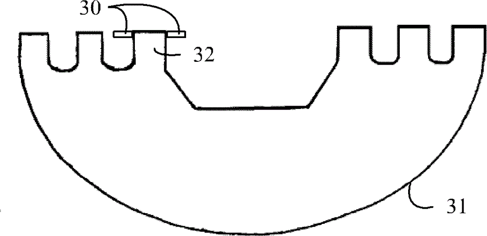
[0035] A preferred embodiment of the present invention provides a method of picking up multiple samples and placing them on a TEM sample holder or TEM grid, which is done to increase throughput in a process that would involve less labor.

[0036] The preferred method or apparatus of the invention has many novel aspects, and since the invention can be embodied in different methods or apparatus for different purposes, it is not necessary to describe every aspect in every embodiment. Furthermore, many aspects of the described embodiments are individually patentable.

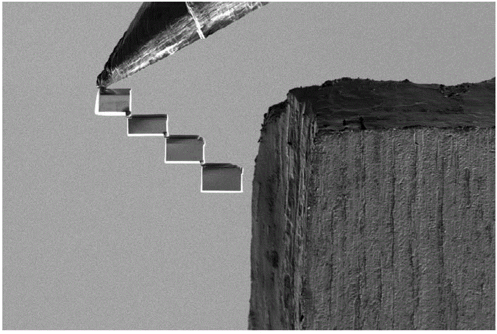
[0037] In a preferred embodiment of the invention, one or more thin layers are first created on a wafer or other substrate. image 3 Shown are a plurality of thin layers 100 that have been ground or machined in preparation for removal from the wafer. Preferably, automated ex-situ processes can be used to create multiple thin layers, as described in "Method for S / TEM Sample Analysis" by Blackwood et al., U.S. Provis...


PUM

PropertyMeasurementUnit
thicknessaaaaaaaaaa

Abstract

An improved method for extracting and handling multiple samples for S / TEM analysis is disclosed. Preferred embodiments of the present invention make use of a micromanipulator that attaches multiple samples at one time in a stacked formation and a method of placing each of the samples onto a TEM grid. By using a method that allows for the processing of multiple samples, the throughput of sample preparation is increased significantly.

Description

technical field [0001] The present invention relates to the extraction and processing of samples for transmission electron microscopy and scanning transmission electron microscopy. Background technique [0002] Semiconductor manufacturing, such as the production of integrated circuits, typically uses photolithography. The semiconductor substrate (usually a silicon wafer) on which the circuitry is formed is coated with a material, such as photoresist, that changes solubility when exposed to radiation. A lithographic tool, such as a mask or reticle, positioned between the radiation source and the semiconductor substrate casts a shadow to control which areas of the substrate are exposed to the radiation. After exposure, the photoresist is removed from either the exposed or unexposed areas, leaving a patterned photoresist layer on the wafer that is subsequently etched or to protect parts of the wafer during the diffusion process. [0003] The photolithographic process allows ...

Claims


Application Information

Patent Timeline
Patent Type & Authority Applications(China)
IPC IPC(8): G01N35/10
CPCG01N1/286H01J37/00H01J2237/208H01J37/3023H01J2237/201G01N1/04H01J2237/31745
Inventor M.施米德特S.斯通C.塞诺维奇
Owner FEI CO
Why Eureka
Eureka Blog
Learn More