
Device for measuring thermal resistance of semiconductor device bottom case to air under thermal coupling effect

A measuring device and semiconductor technology, applied in the direction of material thermal development, etc., can solve the problems of inaccurate thermal resistance network model, affecting the accuracy of temperature rise calculation of semiconductor devices, etc., and achieve the effect of good reliability

Active Publication Date: 2016-09-21
中国东方电气集团有限公司
View PDF7 Cites 0 Cited by
  • Summary
  • Abstract
  • Description
  • Claims
  • Application Information

AI Technical Summary

Problems solved by technology

The traditional thermal resistance measurement device ignores the measurement of the coupling thermal resistance, which leads to the inaccuracy of the established thermal resistance network model, which affects the accuracy of the temperature rise calculation of semiconductor devices

Method used


Image

  • Device for measuring thermal resistance of semiconductor device bottom case to air under thermal coupling effect
  • Device for measuring thermal resistance of semiconductor device bottom case to air under thermal coupling effect
  • Device for measuring thermal resistance of semiconductor device bottom case to air under thermal coupling effect

Examples


Embodiment Construction

[0032] The present invention will be described in further detail below by specific embodiment in conjunction with accompanying drawing:

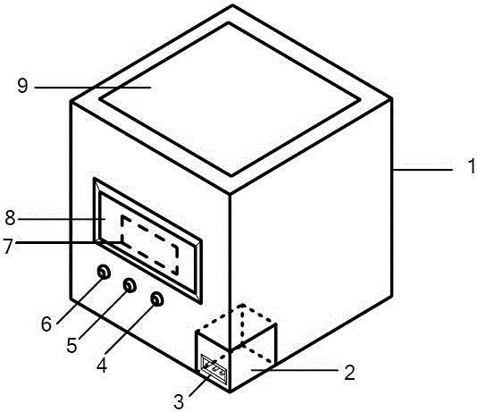
[0033] Such as figure 1 and image 3 As shown, the thermal resistance measurement device from the bottom case of the semiconductor device to the air under the thermal coupling effect of the present invention includes a box body 1, a power supply device 2, an external power supply connection terminal 3, a power button 4, a start button 5, a reset button 6, and a control circuit board 7. Liquid crystal display 8, opening 9 on the top surface of the box, and temperature measuring device 19.

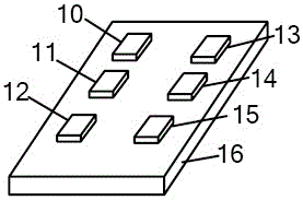
[0034] figure 2 The shown semiconductor devices 10 , 11 , 12 , 13 , 14 , 15 and heat sink 16 are put into the box body 1 through the opening 9 on the top surface of the box body.

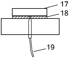
[0035] image 3 indicated by the temperature measuring device 19 on the figure 2 The temperature of the bottom case of one of the semiconductor devices shown is measured,...


PUM


Abstract

The invention discloses a thermal resistance measuring device from the bottom case of a semiconductor device to air under the thermal coupling effect, comprising a plurality of temperature measuring devices for respectively collecting the temperature of the bottom case of the semiconductor device; Measure the semiconductor device and radiator; a control circuit board, used to drive the semiconductor device, and receive the collected temperature of the bottom case of the semiconductor device and calculate the self thermal resistance and coupling thermal resistance; a liquid crystal display, used to display the bottom of the semiconductor device Shell temperature and calculated self-thermal resistance and coupling thermal resistance; a power supply device for providing power consumption to the semiconductor device and the temperature measurement device, control circuit board, and liquid crystal display. The thermal resistance measuring device can conveniently and accurately measure the self thermal resistance and coupling thermal resistance from the bottom case of the semiconductor device to the air under the thermal coupling effect.

Description

technical field [0001] The invention relates to a thermal resistance measuring device from the bottom shell of a semiconductor device to air under the thermal coupling effect, and belongs to the field of measurement and the field of thermal design of devices such as electric energy conversion. Background technique [0002] In a device using semiconductor devices, in order to ensure the reliability of the thermal design of the device, it is usually necessary to use a thermal resistance network to predict the junction temperature of the semiconductor device under actual work or to establish an electrothermal simulation model of the device for dynamic electrothermal co-simulation. Thermal resistance is a very important parameter in the thermal resistance network model. [0003] The thermal resistance from the bottom case to air is included in the total thermal resistance of the semiconductor device mounted on the heat sink. When multiple semiconductor devices are installed on ...

Claims


Application Information

Patent Timeline
Patent Type & Authority Patents(China)
IPC IPC(8): G01N25/20
Inventor 王多平唐健肖文静李琼赵耕边晓光吴建东
Owner 中国东方电气集团有限公司
Learn More