Terminal structure for improving avalanche tolerance of super junction power device

A technology of terminal structure and avalanche tolerance, which is applied in the direction of semiconductor devices, electrical components, circuits, etc., can solve the problems of poor avalanche tolerance, improve reliability, improve avalanche tolerance and reliability, and avoid parasitic BJT conduction problems

Inactive Publication Date: 2014-08-20
UNIV OF ELECTRONICS SCI & TECH OF CHINA
View PDF4 Cites 2 Cited by
  • Summary
  • Abstract
  • Description
  • Claims
  • Application Information

AI Technical Summary

Problems solved by technology

[0006] What the present invention aims to solve is to propose a terminal structure for improving the avalanche tolerance of super-junction power devices in view of the problem of poor avalanche tolerance of traditional super-junction power devices

Method used


Image

  • Terminal structure for improving avalanche tolerance of super junction power device
  • Terminal structure for improving avalanche tolerance of super junction power device
  • Terminal structure for improving avalanche tolerance of super junction power device

Examples


Embodiment Construction

[0023] Below in conjunction with accompanying drawing and embodiment, describe technical solution of the present invention in detail:

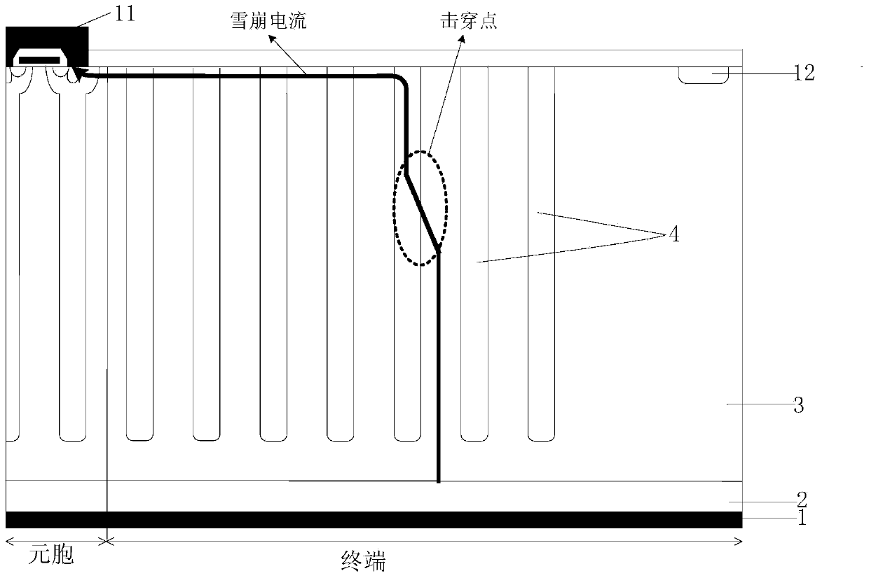
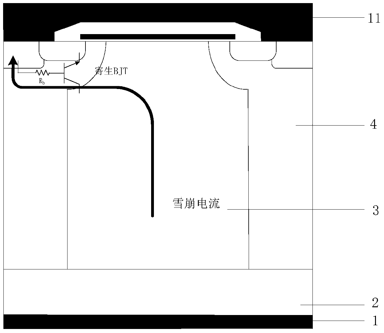
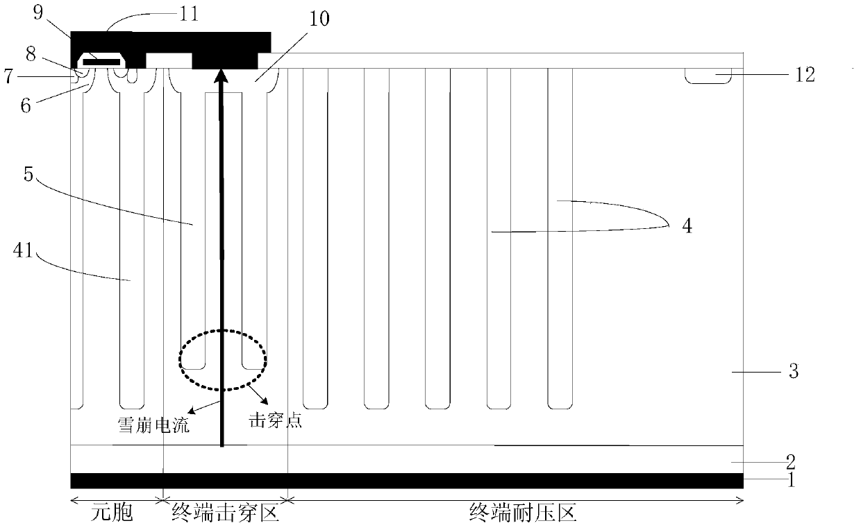
[0024] Such as figure 1 As shown, it is a schematic diagram of the terminal structure of a common super-junction MOSFET. When the avalanche breakdown of the device occurs at the terminal, the location of the breakdown point is random, and the avalanche current will flow from the breakdown point through the terminal surface to the source of the device. The farther the breakdown point is from the element cells, the longer the path of the avalanche current flows. Figure 4 This is the distribution diagram of the avalanche current at the terminal of a common super-junction MOSFET obtained by the simulation tools Tsuprem4 and Medic. It can be seen from the figure that the avalanche current will flow laterally through the surface of the terminal with a long path. The longer the avalanche current path, the greater the resistance of the avalanche cur...


PUM


Abstract

The invention relates to the semiconductor technology, in particular to a terminal structure for improving the avalanche tolerance of a super junction power device. A terminal breakdown region is arranged in a device terminal, avalanche breakdown points are limited in the terminal breakdown region, the parasitic BJT conductivity problem of cellular breakdown is avoided, the problem of local temperature rising caused by the too long path of an avalanche current during common terminal breakdown is avoided, and therefore the avalanche tolerance and reliability of the super junction power device can be improved. The terminal structure has the advantages that the path of the avalanche current is effectively reduced when the device avalanche breakdown points are in the terminal, the anti-UIS lose efficacy capacity of the device is improved on the premise of not affecting the device breakdown voltage, and the reliability of the device is improved. The terminal structure is especially suitable for the super junction power device.

Description

technical field [0001] The invention relates to semiconductor technology, in particular to a terminal structure for improving the avalanche tolerance of super-junction power devices. Background technique [0002] Power MOSFET (Metal Oxide Semiconductor Field Effect Transistor) plays an important role in various power conversions, especially in high-frequency power conversions, due to its advantages of high switching speed, low switching loss, and low driving loss. The switching process under unclamped inductive load (Unclamped InductiveSwitching, UIS) is generally considered to be the most extreme electrical stress situation that power devices can encounter in system applications. Because the energy stored in the inductor must be released by the power device at the moment of turn-off when the loop is turned on, and the high voltage and high current applied to the power device can easily cause the device to fail. Avalanche endurance is an important parameter to measure the a...

Claims


Application Information

Patent Timeline
Patent Type & Authority Applications(China)
IPC IPC(8): H01L29/06H01L29/78
CPCH01L29/0626H01L29/0634H01L29/7838H01L29/7802H01L29/7811
Inventor 任敏姚鑫王为许高潮韩天宇杨珏琳李泽宏张金平高巍张波
Owner UNIV OF ELECTRONICS SCI & TECH OF CHINA
Why Eureka
Try Eureka