
The structure of the chip carrier

A carrier plate and chip technology, which is applied in electrical components, semiconductor/solid-state device manufacturing, circuits, etc., can solve the problem of high cost of double-sided chip carrier, poor process stability of double-sided chip carrier, and poor stacking of chip carrier. And other issues

Active Publication Date: 2017-05-10
SITRONIX TECH CORP
View PDF5 Cites 0 Cited by
  • Summary
  • Abstract
  • Description
  • Claims
  • Application Information

AI Technical Summary

Problems solved by technology

However, the direction of bonding the chip to the substrate will be different for different bonding equipment. For example, the gold bump of the chip must face up and be pressed on the substrate, or the gold bump of the chip must face down and be pressed on the substrate. Therefore, when the chip When the direction of placing the chip on the carrier tray does not match the direction of the lamination equipment to press the chip on the substrate, the operator must first turn all the chips placed on the chip carrier tray and place them upside down on the chip carrier tray, which is very inefficient and time-consuming
Based on this problem, the existing industry has developed double-sided chip carrier trays, but the cost of double-sided chip carrier trays is higher than that of single-sided chip carrier trays
[0006] In order to facilitate transportation and save space, the chip carriers can be stacked on each other, but the chip carriers must be stacked together in a specific stacking direction. The conventional chip carrier does not have a special fool-proof mechanism to prevent the stacking direction from being wrong, so chips are prone to occur. The direction of the tray stack is wrong, and it is easy to cause abnormalities when pressing the chip on the substrate
In addition, after placing the chip on the chip carrier, a protective paper will be placed on the chip carrier to cover the chip, such as Tyvek paper, to protect the chip. However, the conventional chip carrier does not have a structure for fixing the protective paper, so The protective paper is easy to shift. If the protective paper is shifted, it will easily cause poor stacking of the chip carrier tray.
[0007] It can be seen from the above that the conventional chip carrier has the following disadvantages. The first point is that it is not easy for operators to flip the chip from the conventional single-sided chip carrier and place it upside down in the chip carrier, and the error rate is high. It will increase the cost; the second point: the cost of double-sided chip carrier is higher than that of single-sided chip carrier. The stability of the disk manufacturing process is poor; the third point is that the conventional chip carrier does not have a fool-proof mechanism that specifically restricts the stacking direction, so it is easy to cause the chip carrier to stack in the wrong direction; the fourth point is that the conventional chip carrier cannot be fixed and protected paper, the protective paper is easy to shift, and it is easy to cause poor stacking of the chip carrier tray

Method used

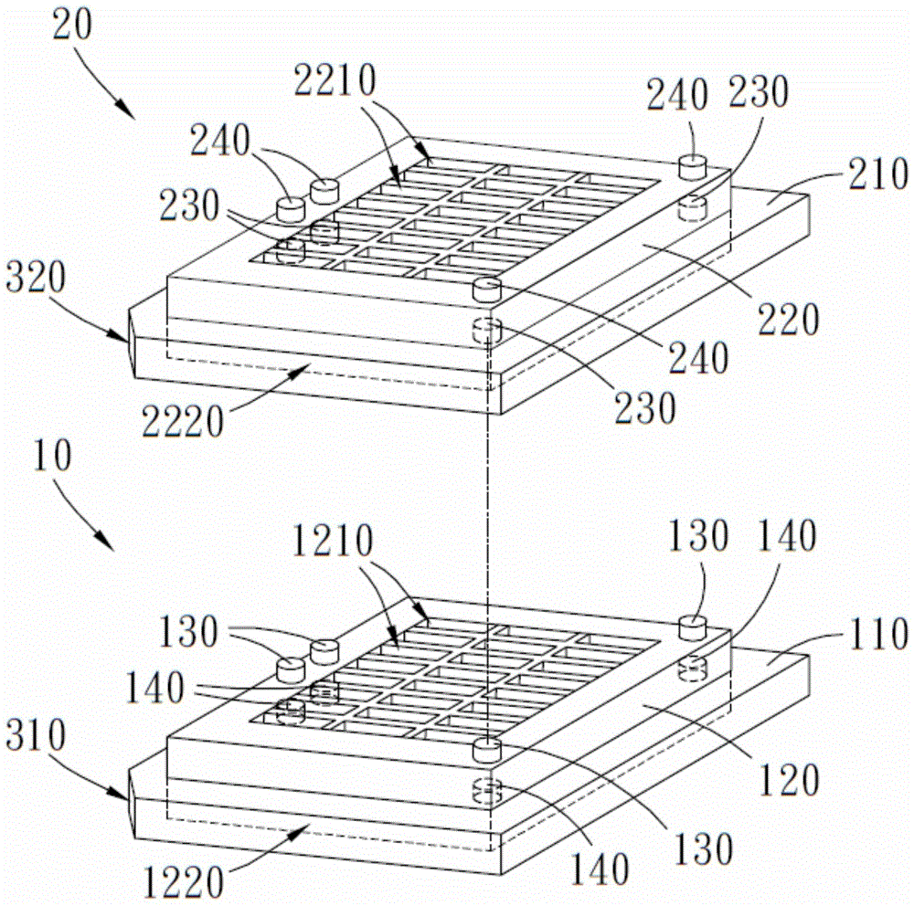
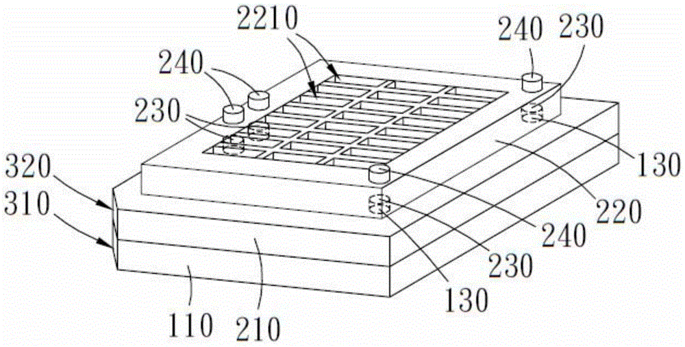
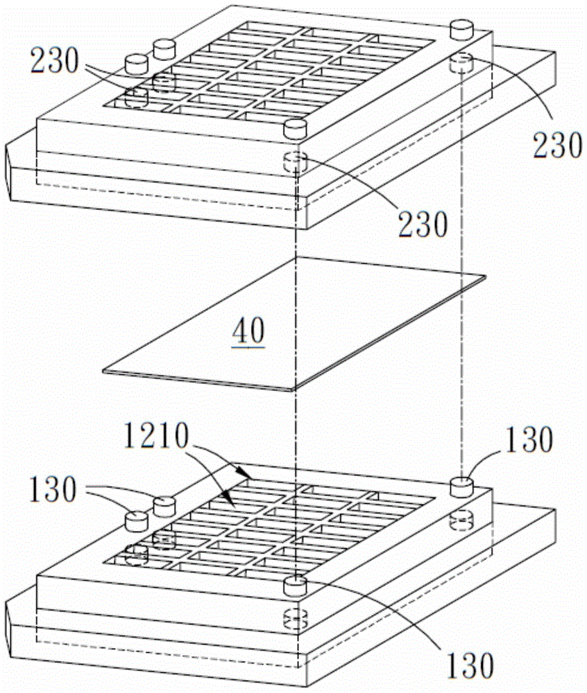

Image

  • The structure of the chip carrier
  • The structure of the chip carrier
  • The structure of the chip carrier

Examples


Embodiment Construction

[0059] In order to make the structural features of the present invention and the achieved effects have a further understanding and recognition, preferred embodiments and detailed descriptions are specially used, which are described as follows:

[0060] The present invention solves the problems related to the structure of the chip carrier in the prior art. In the process of bonding the chip to the substrate, the chip placed in the chip carrier sometimes needs to be turned over and placed upside down in the chip carrier. Flipping the chips one by one manually has a high error rate and is time-consuming, while using a double-sided chip carrier to place the chips costs a lot, and the stability of the manufacturing process of the double-sided chip carrier is poor. In addition, the conventional chip carrier The mechanism for preventing wrong stacking direction of the disc is insufficient, and the conventional chip carrier cannot fix the protective paper on the chip carrier. In order ...


PUM


Abstract

The invention provides a structure of chip bearing discs. The structure is used for containing a plurality of chips. The chip bearing discs are provided with a plurality of inversed alignment pieces, the inversed alignment pieces of the chip bearing disc containing the multiple chips are matched with the inversed alignment pieces of the chip bearing disc without the chips, and the chip bearing disc containing the multiple chips can be overturned to be inversely arranged on the other chip bearing disc so that the chips can be overturned to be really inversely arranged into the other chip bearing disc; in addition, the chip bearing discs are further provided with a plurality of stacking alignment pieces, the stacking alignment pieces are arranged on the chip bearing discs in an asymmetric mode to assist in stacked alignment of the multiple bearing discs, and the stacking direction of the stacked bearing discs is limited.

Description

technical field [0001] The present invention relates to a chip carrier, in particular to a structure of the chip carrier which is beneficial to flip-chip alignment and stack alignment. Background technique [0002] In the general chip (IC) manufacturing process, the carrier tray is usually used to place the chip. The carrier tray has multiple accommodating slots for placing the chip, so the IC tray (IC Tray) is used in the back-end process of the chip and transports the chip to the client. The above is an important holding container. [0003] Chip on Glass (COG) is an advanced packaging technology that connects chips and substrates. Using flip chip (Flip Chip) technology, with anisotropic conductive film (ACF) as the intermediate interface, there will be gold The chip of the bump is bonded on the substrate; when it is applied to a liquid crystal display, it is called COG because the substrate is glass. The chip manufacturing process includes grinding, dicing, picking, visu...

Claims


Application Information

Patent Timeline
Patent Type & Authority Patents(China)
IPC IPC(8): H01L21/673H01L21/68
CPCH01L21/67326
Inventor 陈柏琦
Owner SITRONIX TECH CORP
Learn More