Method for Improving Device Negative Bias Temperature Instability

A negative bias temperature and instability technology, used in semiconductor devices, semiconductor/solid-state device manufacturing, electrical components, etc., can solve the effects of negative bias temperature instability, threshold voltage drift, weak gate control capabilities, etc. The problem is to improve the temperature instability of negative bias voltage, reduce the drift of threshold voltage, and reduce the generation of H+

Active Publication Date: 2017-05-24
SHANGHAI HUALI MICROELECTRONICS CORP
View PDF6 Cites 0 Cited by
  • Summary
  • Abstract
  • Description
  • Claims
  • Application Information

AI Technical Summary

Problems solved by technology

[0003] In the existing manufacturing process, the gate oxide layer (Gate 1 oxide) adopts a Wet deposition process. During the process, H is introduced to form H+, which drifts toward the gate under the action of the gate electric field. Some It will be trapped by oxide layer defects to form positive oxide trap charges. This part of the charge will cause the threshold voltage to shift, and the gate control ability will become weak. Under the same gate voltage and drain voltage, the degree of inversion layer is reduced, and the saturation current decrease, the driving energy of the device decreases; another part of H+ will continue to interact with the Si-H bond at the interface to make Si-H decompose and form H2, leaving the interface trap that is the dangling bond of trivalent silicon, and the generation of interface trap will lead to The increase of the surface scattering rate, thus affecting the carrier mobility, transconductance, etc.
As a result, the negative bias temperature instability NBTI (Negative bias temperature instability) of the device is affected

Method used


Image

  • Method for Improving Device Negative Bias Temperature Instability

Examples


Embodiment Construction

[0014] In order to make the content of the present invention clearer and easier to understand, the content of the present invention will be described in detail below in conjunction with specific embodiments and accompanying drawings.

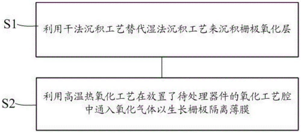
[0015] In the reliability analysis of semiconductor devices, the negative bias temperature instability NBTI (Negative bias temperature instability) is a very important consideration parameter, aiming at improving the negative bias temperature instability NBTI of the device, the present invention adds In the deposition process, dry oxidation is used instead of wet deposition, and chlorine-doped HTO (thermal oxidation) is used for the growth of gate spacers, thereby reducing the generation of H+ and reducing the number of trapped charges in the positive oxide layer , improving the negative bias temperature instability NBTI of the device.

[0016] Specifically, by changing the wet deposition of the gate oxide layer deposition process in the existin...


PUM


Abstract

The invention provides a method for avoiding negative bias temperature instability of a device. The method includes the steps that a wet method deposition process is utilized to replace a dry method deposition process to deposit a grid electrode oxidation layer; after the grid electrode oxidation layer is deposited, oxidizing gas is fed into an oxidation process cavity in which the device to be processed is placed through a high-temperature heat oxidation process so that a grid electrode isolation film can grow. When the grid electrode isolation film grows through the high-temperature heat oxidation process, dichlorosilane is mixed into the oxidizing gas, and then the high-temperature heat oxidation process of the grid electrode isolation film can be finished.

Description

technical field [0001] The invention relates to the field of semiconductor manufacturing, and more specifically, the invention relates to a method for improving the temperature instability of negative bias voltage of devices by improving furnace tube technology. Background technique [0002] When the PMOS device is working, when the gate is under negative bias, after a certain period of time, the absolute value of the threshold voltage of the device will continue to increase, and the drain current and transconductance will continue to decrease. This effect will increase with the bias voltage increase more significantly. [0003] In the existing manufacturing process, the gate oxide layer (Gate 1 oxide) adopts a Wet deposition process. During the process, H is introduced to form H+, which drifts toward the gate under the action of the gate electric field. Some It will be trapped by defects in the oxide layer to form trap charges in the positive oxide layer. This part of the ...

Claims


Application Information

Patent Timeline
Patent Type & Authority Patents(China)
IPC IPC(8): H01L21/28H01L21/285
CPCH01L21/28211H01L21/28229H01L21/285
Inventor 朱双龙胡鹏超刘景富
Owner SHANGHAI HUALI MICROELECTRONICS CORP
Why Eureka
Try Eureka