A semiconductor laser with high power and high beam quality laser

A semiconductor and high-beam technology, which is applied to the device for controlling the output parameters of the laser, the structure of the optical resonator, etc., can solve the problems of affecting the quality of the laser beam, the ineffective application, and the deterioration of the beam quality, so as to expand the application range and reduce the size of the laser beam. Spot, improve the effect of the mode

Active Publication Date: 2017-06-23
华芯半导体科技有限公司
View PDF5 Cites 2 Cited by
  • Summary
  • Abstract
  • Description
  • Claims
  • Application Information

AI Technical Summary

Problems solved by technology

However, as the output power of the laser increases, factors such as thermal effects will gradually be amplified, thereby affecting the beam quality of the laser. Therefore, the beam quality and power of the laser have always been in opposition to each other. When developing a laser, the pros and cons of practical applications must be weighed. A trade-off between these two parameters
[0003] Compared with other types of lasers (such as gas lasers and solid-state lasers), semiconductor lasers have higher electro-optical efficiency (no fiber coupling loss or secondary pump loss), low cost (no expensive high-power energy transmission fibers), etc. advantages, but its beam quality will seriously deteriorate with the increase of laser output power, how to effectively expand the output power of semiconductor lasers under the premise of maintaining beam quality has always been a research hotspot in this field
[0004] Semiconductor laser array (bar) technology is a very convenient semiconductor laser power expansion technology. Its principle is to arrange several semiconductor light-emitting units in parallel on the substrate so that the output power of the laser increases linearly with the number of light-emitting units. However, due to The near-field wavefront of the laser beam obtained by this method is divided, so the beam quality is very poor, and it cannot be effectively applied to technical fields such as fiber coupling, welding, and cutting that require high-beam quality lasers.

Method used


Image

  • A semiconductor laser with high power and high beam quality laser
  • A semiconductor laser with high power and high beam quality laser
  • A semiconductor laser with high power and high beam quality laser

Examples


Embodiment 1

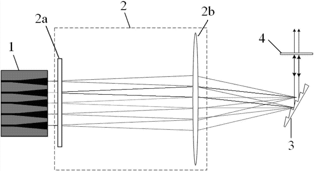
[0023] figure 1 The structure and optical path of a semiconductor laser with high power and high beam quality laser according to the embodiment of the present invention are shown. In this embodiment, the semiconductor gain medium is (InGa)(AsP) / InP, and its semiconductor gain element 1 contains 19 active gain regions, each of which is cone-shaped to reduce its The transverse mode of the output laser results in better beam quality. The rear surface is coated with a high reflectance film to 940nm±5nm, and the front surface is coated with a high transmittance film to 940nm±5nm. The coupling output mirror 4' is a concave mirror coated with a film with a transmittance of 80%. The light beam emitted by the active gain area passes through the cylindrical lens 2a and the spherical lens 2b to collimate the fast axis and the slow axis respectively, and then is collimated by the spherical lens 2b. Focused on the blazed grating 3, after being reflected, the light beam is partially trans...

Embodiment 2

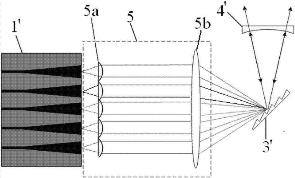
[0028] figure 2 It shows the structure and optical path of the semiconductor laser with high power and high beam quality laser in the second embodiment of the present invention. In this embodiment, the semiconductor gain medium is (InGa)(AsP) / InP, and its semiconductor gain element 1' contains 19 active gain regions, and each active gain region is conical in shape to reduce It outputs the transverse mode of the laser light, resulting in better beam quality. The rear surface is coated with a high reflectance film to 940nm±5nm, and the front surface is coated with a high transmittance film to 940nm±5nm. The coupling output mirror 4 is a flat mirror coated with a film with a transmittance of 80%. The light beam emitted by the active gain area is collimated by the microlens 5a, focused by the spherical lens 5b and irradiated onto the blazed grating 3', and then coupled The output mirror 4' partly transmits the output and partly feeds back the oscillation. If the first-order di...


PUM


Abstract

A semiconductor laser with high-power and high-beam-quality lasers. An external resonant cavity is built outside the semiconductor gain element, and a collimating optical element, a spectral dispersion element, and a coupling output mirror are sequentially arranged in the external resonant cavity. The semiconductor gain element consists of several active gain regions arranged in parallel in a straight line. One side of each active gain region is coated with a film layer with high reflectivity to the laser wavelength, and the other side is coated with a film layer with high transmittance to the laser wavelength. film layer. The collimating optical element is located behind the side of the semiconductor gain element coated with a high-transmittance film layer, and its central optical axis coincides with the central optical axis of the light beam emitted by the semiconductor optical gain element. The spectral dispersing element is placed at an angle behind the collimating optics. The outcoupling mirror is located behind the spectral dispersion element along the beam propagation direction. The invention improves the mode of laser oscillation and effectively increases the output power of the laser without affecting the quality of the laser beam.

Description

technical field [0001] The invention relates to a power expansion technology of an external cavity semiconductor laser, in particular to a semiconductor laser with high power and high beam quality laser. Background technique [0002] Due to its high brightness, good monochromaticity, good collimation and focusing performance, laser has been widely used in scientific research, military defense, industrial processing, astronomical observation and information dissemination and other fields. The beam quality of the laser is a parameter that describes the focusing and collimation capabilities of the laser during propagation. A laser with high beam quality will get a smaller spot after focusing and a smaller far-field divergence angle after collimation. Therefore, in practice In applications, lasers with high beam quality have always been the direction people are pursuing. However, as the output power of the laser increases, factors such as thermal effects will gradually be ampli...

Claims


Application Information

Patent Timeline
Patent Type & Authority Patents(China)
IPC IPC(8): H01S5/14H01S5/06
Inventor 邱运涛尧舜曹银花王智勇秦文斌
Owner 华芯半导体科技有限公司
Why Eureka
Try Eureka