How to make through silicon vias

A manufacturing method and technology of through-silicon vias, which are applied in the manufacture of microstructure devices, processes for producing decorative surface effects, decorative arts, etc., can solve the problem of high contact resistance between pure polysilicon fillers and connecting lines, and reliability of thermal expansion coefficient devices. Reduction and other problems, to achieve high density, low contact resistance, and solve the effect of large contact resistance

Active Publication Date: 2016-01-06
SHANGHAI INST OF MICROSYSTEM & INFORMATION TECH CHINESE ACAD OF SCI
View PDF7 Cites 0 Cited by
  • Summary
  • Abstract
  • Description
  • Claims
  • Application Information

AI Technical Summary

Problems solved by technology

[0006] In view of the above-mentioned shortcomings of the prior art, the object of the present invention is to provide a method for manufacturing through-silicon vias, which is used to solve the difference in thermal expansion coefficient between the metal filling and silicon formed by the deposition method during the manufacture of through-silicon vias in the prior art. The lower reliability of the device caused by the deposition and the large contact resistance between the pure polysilicon filling and the wiring

Method used


Image

  • How to make through silicon vias
  • How to make through silicon vias
  • How to make through silicon vias

Examples


Embodiment 1

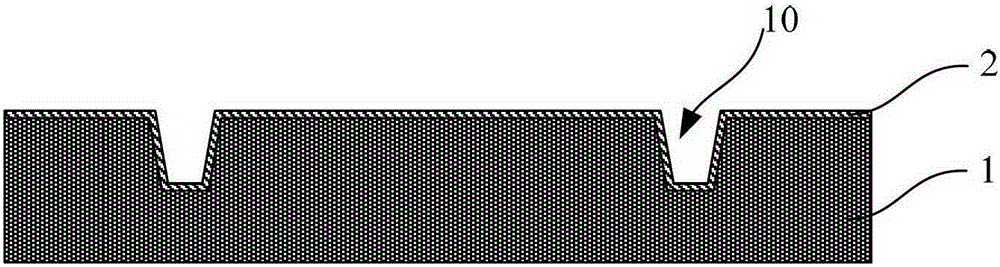
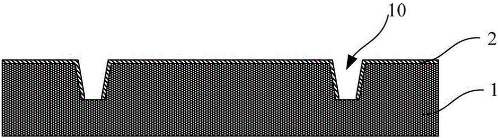
[0044] like Figure 1A to Figure 1M As shown, the present invention provides a method for manufacturing through-silicon vias, which at least includes the following steps:

[0045] Firstly, step 1) is performed to provide a substrate 1 , and the groove 10 is formed by dry etching or wet etching at the place where the TSV is prefabricated in the substrate 1 . Wherein, the dry etching includes at least reactive ion etching (ReactiveIonEtching, RIE) or inductively coupled plasma (InductiveCoupledPlasma, ICP), and the wet etching includes at least using potassium hydroxide solution; the material of the substrate 1 is Silicon; the shape of the opening of the groove 10 is circular or square, the size of the opening is 80-150 μm, and the aspect ratio of the groove 10 ranges from 1 to 5; the angle between the side wall of the groove 10 and the opening depends on For the method of making the groove, the angle between the side wall of the groove 10 and the opening can be approximately 9...

Embodiment 2

[0059] Embodiment 2 adopts basically the same technical solution as Embodiment 1. The difference is that the manufacturing method of through-silicon vias in this embodiment 2 is applicable to the case where through-silicon vias realize the electrical connection of MEMS devices. The specific difference is reflected in step 4. ), which will be described in detail later.

[0060] like Figure 2A to Figure 2H As shown, the present invention provides a method for manufacturing through-silicon vias, and the manufacturing method at least includes:

[0061] First perform the same steps 1)~3) as in Example 1, such as Figure 2A~2D As shown, a groove 10' filled with an epitaxial layer 3' of silicon material and an insulating layer 2' formed on a side wall is made on a substrate 1'. Wherein, the groove 10' corresponds to the prefabricated TSV; the insulating layer 2' is formed on the side wall of the groove 10' but there is no insulating layer 2' at the bottom of the groove 10'; The e...


PUM

PropertyMeasurementUnit
thicknessaaaaaaaaaa

Abstract

The invention provides a preparation method for through-silicon via. An insulating layer is formed on the upper surface of a base plate with formed grooves, and the grooves correspond to pre-prepared through-silicon vias; then a silicon material epitaxial layer is grown on the surface of the insulating layer until the grooves are filled, and then the epitaxial layer is thinned until the insulating layer on the upper surface of the base plate is exposed; and then the reverse side of the base plate is thinned until the grooves are exposed, so that the through-silicon vias filled with the epitaxial layer and the insulating layer are formed. By employing the epitaxially grown silicon material for filling the through-silicon vias, on the one hand, the filler in the through-silicon vias are extremely high in compactness and the reliability of an appliance is improved, and on the other hand, the problem is effectively solved that the reliability of the appliance is reduced because of the thermal expansion coefficient difference between the filler and silicon. Also, the epitaxial layer filler of the through-silicon vias comprises monocrystal silicon, thereby solving the problem of relatively large contact resistance of a connection part between a redistribution layer and the filler when only polysilicon is used for filling.

Description

technical field [0001] The invention adopts microelectronic machining technology, belongs to the field of microelectromechanical systems, and relates to a method for manufacturing a through-silicon hole, in particular to a method for manufacturing a through-silicon hole applied to the electrical connection of devices. Background technique [0002] Through-silicon via technology is the abbreviation of Through Silicon Via (TSV) technology, which is the latest technology to realize the interconnection between chips by making vertical conduction between chips and between wafers and wafers. In the packaging process of Micro Electro Mechanical Systems (MEMS) devices, through-silicon via technology can also be used to realize the electrical connection between multiple layers of devices. [0003] StevenS.Nasiri and AnthonyFrancisFlannery, JR. proposed a CMOS silicon chip and MEMS silicon chip bonding and packaging structure using through-silicon vias (Method off abrication of Al / Geb...

Claims


Application Information

Patent Timeline
Patent Type & Authority Patents(China)
IPC IPC(8): B81C1/00
Inventor 焦继伟王敏昌
Owner SHANGHAI INST OF MICROSYSTEM & INFORMATION TECH CHINESE ACAD OF SCI
Why Eureka
Try Eureka