Enhanced type, depletion type and current induction integrated VDMOS power device
A technology for current sensing and power devices, applied in the field of VDMOS power devices, can solve problems such as hindering product miniaturization, complex manufacturing process, and large occupied area, and achieve the effect of being conducive to miniaturization, low manufacturing cost and low cost
- Summary
- Abstract
- Description
- Claims
- Application Information
AI Technical Summary
Problems solved by technology
Method used
Image
Examples
Embodiment Construction
[0015] The present invention will be further described below in conjunction with the accompanying drawings and embodiments.
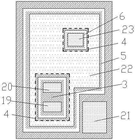
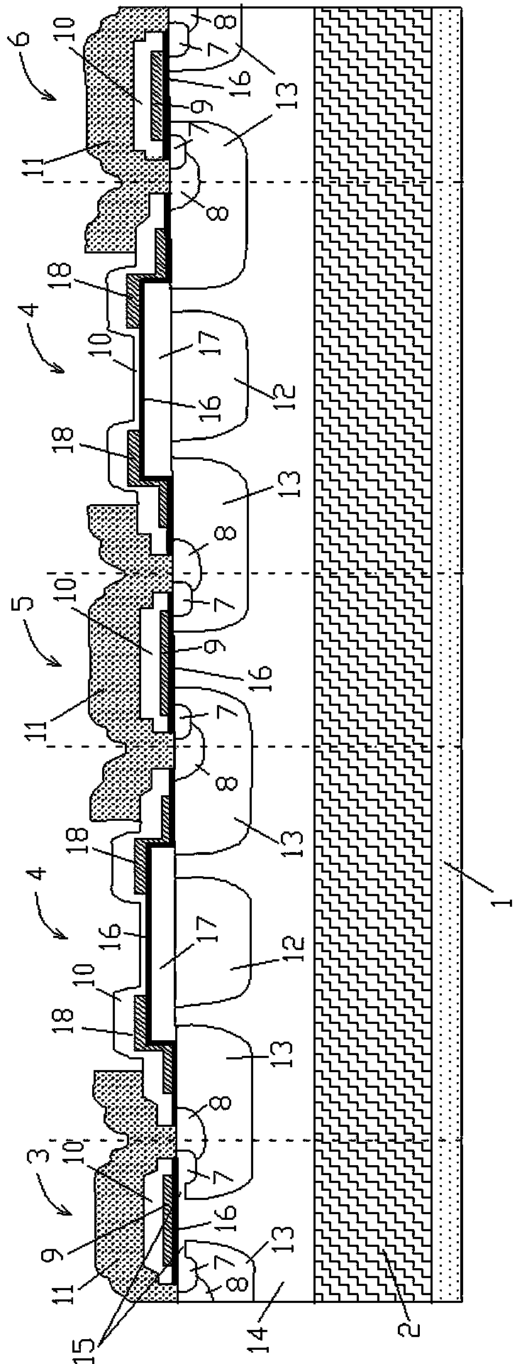
[0016] Such as figure 1 As shown, the present embodiment provides an enhanced, depleted and current-sensing integrated VDMOS power device, including an N-type substrate 2, and an N-type epitaxial layer 14 is arranged on the N-type substrate 2, and is characterized in that: The N-type epitaxial layer 14 is provided with an enhanced VDMOS5, a depletion-type VDMOS3, a current-sensing VDMOS6 and two isolation structures 4, wherein the three types of VDMOS devices share a drain, and the enhanced-type VDMOS and the current-sensing VDMOS share a gate, so The isolation structure 4 is respectively arranged between the sources of the enhancement VDMOS, the depletion VDMOS and the current sensing VDMOS. The gate of the enhanced VDMOS and the gate of the current sensing VDMOS are commonly connected to a common gate through a metal;
[0017] Please continue to see...
PUM
 Abstract
Description
Claims
Application Information
 - R&D
- Intellectual Property
- Life Sciences
- Materials
- Tech Scout
- Unparalleled Data Quality
- Higher Quality Content
- 60% Fewer Hallucinations
Browse by: Latest US Patents, China's latest patents, Technical Efficacy Thesaurus, Application Domain, Technology Topic, Popular Technical Reports.
© 2025 PatSnap. All rights reserved.Legal|Privacy policy|Modern Slavery Act Transparency Statement|Sitemap|About US| Contact US: help@patsnap.com


