Interconnect structure and method of forming the same

A technology of interconnection lines and interlayer dielectric layers, applied in the field of interconnection line structure and its formation, can solve problems such as poor quality, complicated manufacturing process, and large stack thickness, so as to achieve improved quality, low process cost, and reduced Effect of small stack thickness

Active Publication Date: 2016-11-02
SHANGHAI HUAHONG GRACE SEMICON MFG CORP
View PDF7 Cites 0 Cited by
  • Summary
  • Abstract
  • Description
  • Claims
  • Application Information

AI Technical Summary

Problems solved by technology

[0011] To sum up, it can be seen that the formation method of the existing interconnection structure is complex and the manufacturing process is complicated, and the lamination thickness of the existing interconnection structure is large and the quality is not good.

Method used


Image

  • Interconnect structure and method of forming the same
  • Interconnect structure and method of forming the same
  • Interconnect structure and method of forming the same

Examples


Embodiment Construction

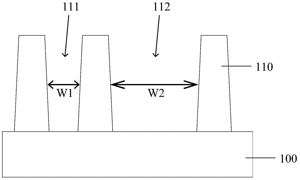
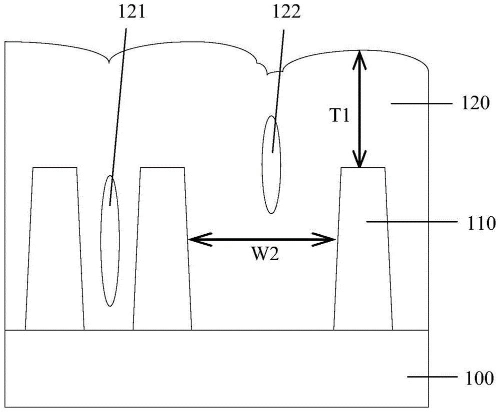
[0039] It can be seen from the description of the background technology that in the existing method for forming the interconnect structure, when the first interlayer dielectric layer is filled with a larger width (for example figure 1 and figure 2 In the case of a trench with a width W2), an air gap at a higher position (relative to the upper surface of the interconnect structure) will be formed. In order to prevent the air gap from causing bubble defects on the upper surface of the interconnect structure, the first interlayer dielectric The thickness of the layer is usually large, and a second interlayer dielectric layer with the same thickness needs to be formed on the first interlayer dielectric layer. In addition, after the second interlayer dielectric layer is planarized, it is also necessary to The protective layer is formed on the dielectric layer, and the whole forming method is complex in process and high in process cost, and the quality of the formed interconnection...


PUM


Abstract

The invention relates to an interconnecting wire structure and a forming method thereof. A semiconductor substrate is provided; the forming method of the interconnecting wire structure comprises the steps of forming multiple independent interconnecting wires on the semiconductor substrate, wherein grooves are formed between adjacent interconnecting wires; forming a first interlayer dielectric layer to cover the interconnecting wires, and filling a groove in part of the first interlayer dielectric layer until an opening is formed; forming a second interlayer dielectric layer to cover the first interlayer dielectric layer, wherein the opening is sealed by the second interlayer dielectric layer to form an air gap; flattening the second interlayer dielectric layer. The interconnecting wire structure formed by the forming method is improved in quality, and the forming method is simple in process and low in process cost.

Description

technical field [0001] The invention relates to the field of semiconductor manufacturing, in particular to an interconnect structure and a forming method thereof. Background technique [0002] One of the challenges encountered in the field of integrated circuit design and manufacturing today is how to reduce the RC delay (Resistance Capacitance Delay) of signal transmission. In this regard, a commonly used method is to reduce the parasitic capacitance (Parasitic Capacitance) between interconnection structures. . [0003] Generally, the interlayer dielectric layer (Inter Layer Dielectric) can be made by using a dielectric layer with a low dielectric constant, thereby reducing the RC delay of signal transmission. Since the dielectric constant of air is low, close to 1.0 (relative dielectric constant value), an air gap (Air Gap) can be formed in the interlayer dielectric layer, thereby greatly reducing the dielectric constant of the interlayer dielectric layer. [0004] Pleas...

Claims


Application Information

Patent Timeline
Patent Type & Authority Patents(China)
IPC IPC(8): H01L21/768H01L23/522H01L23/528
Inventor 蒙飞李乐
Owner SHANGHAI HUAHONG GRACE SEMICON MFG CORP
Why Eureka
Try Eureka