Organic electroluminescence device with quantum well structure and preparation method thereof

A quantum well and electroluminescence technology, which is applied in the field of electric light sources, can solve the problems of reduced recombination probability of holes and electrons, short lifespan of OLEDs and high starting voltage, and achieves the effects of simple process, improved production efficiency and uniform structure

Inactive Publication Date: 2014-06-11
OCEANS KING LIGHTING SCI&TECH CO LTD +2
View PDF3 Cites 9 Cited by
  • Summary
  • Abstract
  • Description
  • Claims
  • Application Information

AI Technical Summary

Problems solved by technology

[0004] However, it has been found through research that in traditional light-emitting devices, the hole transport rate is generally higher than the electron transport rate by more than two orders of magnitude, which causes a large number of holes to accumulate in the light-emitting region, while the number of electrons is small, which eventually leads to holes and electrons. The recombination probability of electrons is greatly reduced, resulting in low luminous efficiency
In addition, at present, OLED still needs high starting voltage and high current, which leads to short life of OLED. In order to realize the practical application of organic electroluminescent devices, people are eager to find a light-emitting device structure with small driving current and high luminous efficiency.

Method used


Image

  • Organic electroluminescence device with quantum well structure and preparation method thereof
  • Organic electroluminescence device with quantum well structure and preparation method thereof
  • Organic electroluminescence device with quantum well structure and preparation method thereof

Examples


preparation example Construction

[0038] The embodiment of the present invention also provides a preparation method of the above-mentioned organic electroluminescent device containing the quantum well structure based on the above principle, the process flow chart of the method is as follows Figure 4 Therefore, see also Figure 1~3 , the method includes the following steps:

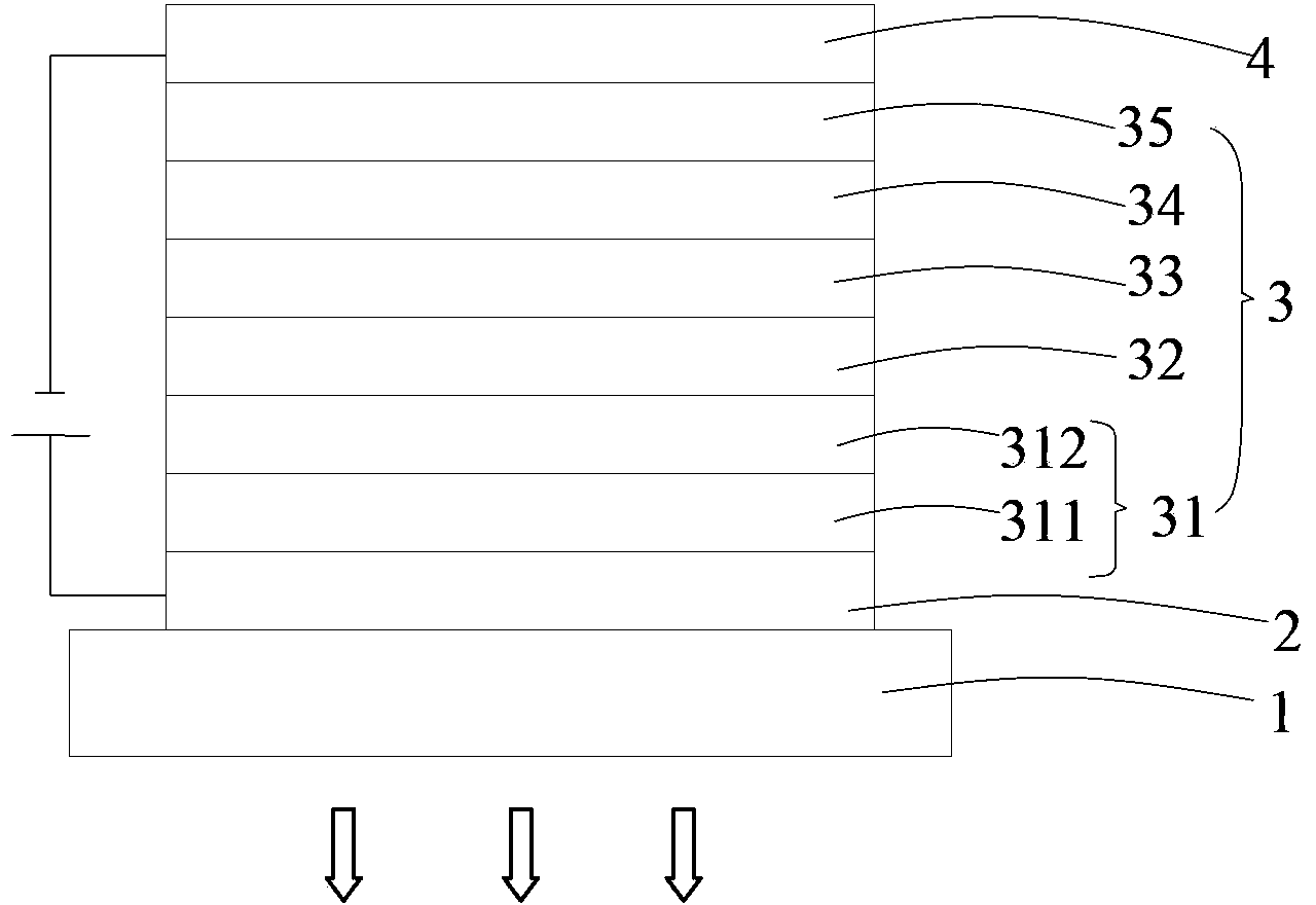
[0039] S01: providing a substrate layer 1;

[0040] S02: Prepare the anode layer 2: plate the anode layer 2 on the surface of the substrate layer 1 in step S01;

[0041] S03: Preparation of organic functional layer 3: In step S02, the surface of the anode layer 2 opposite to the substrate layer 1 is prepared and plated with a hole transport layer 31, an electron blocking layer 32, a light emitting layer 33, an electron transport layer 34, and an electron injection layer in sequence. Layer 35, forming an organic functional layer 3; wherein, the hole transport layer 31 is the quantum well structure described above;

[0042] S04: Preparin...

Embodiment 1

[0060] An organic electroluminescence device containing a quantum well structure, the structure of which is a glass substrate / ITO (100nm) / ReO 3 (0.5nm) / NPB(10nm) / TAPC(10nm) / TCTA:Ir(MDQ) 2 (acac)(25nm) / BAlq(10nm) / TPBi(20nm) / LiF(0.5nm) / Al(100nm).

[0061] Among them, ITO / ReO 3 / NPB consists of a quantum well structure with a period of 1, namely the hole transport layer, the TPAC layer is the electron blocking layer, TCTA:Ir(MDQ) 2 The (acac) layer is the light-emitting layer, the BAlq layer is the hole blocking layer, the TPBi layer is the electron transport layer, the LiF layer is the electron injection layer, and the Al layer is the cathode.

[0062] The method for preparing an organic electroluminescence device containing a quantum well structure comprises the following steps:

[0063] Step S11. Provide a glass substrate: place the glass substrate in deionized water containing detergent for ultrasonic cleaning, and after cleaning, use isopropanol and acetone in ultrasonic ...

Embodiment 2

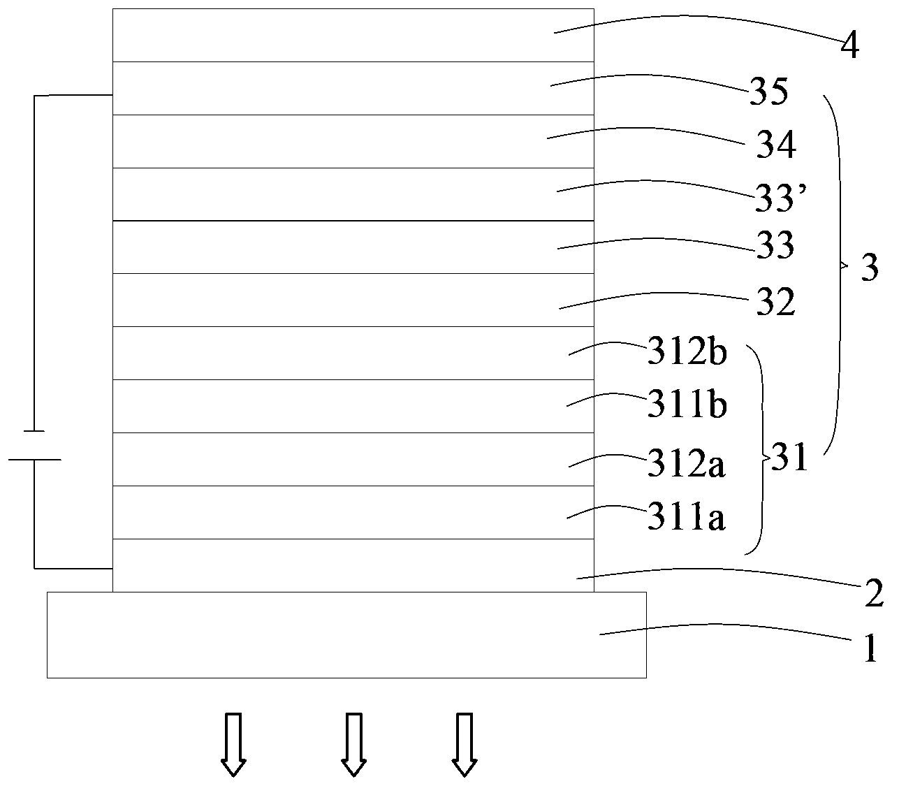
[0069] An organic electroluminescent device containing a quantum well structure, the structure of which is a glass substrate / ITO (100nm) / Re 2 o 7 (1nm) / 2-TNATA(15nm) / Re 2 o 7 (1nm) / 2-TNATA(15nm) / TAPC(10nm) / TCTA:Ir(MDQ) 2 (acac)(25nm) / BAlq(10nm) / TPBi(20nm) / LiF(0.5nm) / Al(100nm).

[0070] Among them, ITO(100nm) / Re 2 o 7 (1nm) / 2-TNATA(15nm) / Re 2 o 7 (1nm) / 2-TNATA consists of a quantum well structure with a period of 2, that is, the hole transport layer, and the TPAC layer is the electron blocking layer, TCTA:Ir(MDQ) 2 The (acac) layer is the light-emitting layer, the BAlq layer is the hole blocking layer, the TPBi layer is the electron transport layer, the LiF layer is the electron injection layer, and the Al layer is the cathode.

[0071] The method for preparing an organic electroluminescence device containing a quantum well structure comprises the following steps:

[0072] Step S21. Providing a glass substrate: refer to step S11 in Embodiment 1;

[0073] Step S22. In ...


PUM


Abstract

The invention discloses an organic electroluminescence device with a quantum well structure and a preparation method thereof. The organic electroluminescence device with the quantum well structure comprises a light-transmitting substrate layer, an anode layer, an organic functional layer and a cathode layer which are laminated and combined in turn. The organic functional layer comprises a hole transmission layer and a light-emitting layer which is driven to emit light by an external power supply. The hole transmission layer is laminated and combined between the anode layer and the light-emitting layer. The hole transmission layer is the quantum well structure, and an inorganic oxide layer acts as a potential well, an organic hole transmission material layer acts as a potential barrier and HOMO energy level of organic hole transmission material is higher than Fermi energy level of inorganic oxide. The hole transmission layer of the organic electroluminescence device is arranged to be the quantum well structure so that hole carrier concentration and conductivity are effectively enhanced, ohmic contact is formed between the anode layer and the hole transmission layer, and driving voltage of the device is reduced. Technology of a preparation method of the organic electroluminescence device is easy to control so that production efficiency is high and the organic electroluminescence device is suitable for industrialized production.

Description

technical field [0001] The invention belongs to the technical field of electric light sources, and in particular relates to an organic electroluminescent device with a quantum well structure and a preparation method thereof. Background technique [0002] Organic Light Emission Diode (hereinafter referred to as OLED) has the characteristics of high brightness, wide range of material selection, low driving voltage, full-cured active light emission, etc., and has the advantages of high definition, wide viewing angle, and fast response speed. A display technology and light source with great potential, in line with the development trend of mobile communication and information display in the information age, and the requirements of green lighting technology, is the focus of many researchers at home and abroad. [0003] The principle of OLED light emission is based on the action of an external electric field, electrons are injected from the cathode to the lowest unoccupied molecula...

Claims


Application Information

Patent Timeline
Patent Type & Authority Applications(China)
IPC IPC(8): H01L51/50H01L51/56
CPCH10K85/6572H10K50/15
Inventor 周明杰王平冯小明张振华
Owner OCEANS KING LIGHTING SCI&TECH CO LTD
Why Eureka
Try Eureka