Back channel etching oxide thin film transistor process architecture

A technology of oxide thin film and back channel, which is applied in the field of back channel etching oxide thin film transistor process architecture, which can solve the problems of increasing production time, reducing output, and interrupting conductive materials

Inactive Publication Date: 2014-05-14
APPLE INC
View PDF5 Cites 6 Cited by
  • Summary
  • Abstract
  • Description
  • Claims
  • Application Information

AI Technical Summary

Problems solved by technology

Often, very different etch rates between the passivation layer and the gate insulator create undercuts in the vias, which can lead to interruptions in the conductive material used to coat the vias, thereby interfering with the operation of the TFT
[0007...

Method used


Image

  • Back channel etching oxide thin film transistor process architecture
  • Back channel etching oxide thin film transistor process architecture
  • Back channel etching oxide thin film transistor process architecture

Examples


Embodiment Construction

[0041] The present disclosure can be understood by referring to the following detailed description in conjunction with the accompanying drawings described below. Note that for clarity of illustration, some elements in the various figures may not have been drawn to scale.

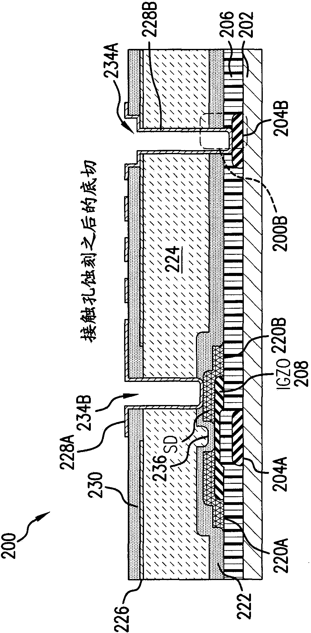
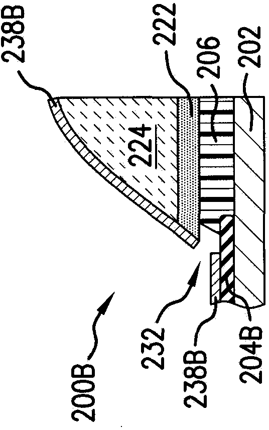
[0042] Figure 2A A cross-sectional view of an oxide TFT for an AMLCD according to an embodiment of the present disclosure is shown. The oxide TFT 200 includes a substrate 202 , a first metal layer disposed on the substrate 202 including a gate electrode 204A and a metal common electrode 204B. The oxide TFT 200 also includes a gate insulator 206 disposed on the gate electrode 204A and the metal common electrode 204B. Oxide TFT 200 also includes a semiconductor such as IGZO layer 208 disposed on gate insulator 206 above gate electrode 204A. The oxide TFT 200 also has a second metal layer including a source electrode 220A and a drain electrode 220B provided on the IGZO 208 . The source and drain electrodes...


PUM


Abstract

The disclosure relates to a back channel etching oxide thin film transisto process architecture. A method for fabricating a back channel etching (BCE) oxide thin film transistor (TFT) for a liquid crystal display is provided. The method includes forming a first metal layer having a first portion and a second portion over a substrate, depositing a gate insulator over the first metal layer, and disposing a semiconductor layer over the gate insulator. The method also includes depositing a half-tone photoresist to cover a first portion of the semiconductor layer and the first portion of the first metal layer. The half-tone photoresist has a first portion and a second portion thicker than the first portion. The first portion has a through hole above the second portion of the first metal layer. The second portion of the half-tone photoresist covers the first portion of the first metal layer. The method further includes etching a portion of the gate insulator through the via hole such that the second portion of the first metal layer is exposed, removing the first portion of the half-tone photoresist while remaining the second portion of the half-tone photoresist, and etching to remove a second portion of the semiconductor layer that is not covered by the half-tone photoresist.

Description

[0001] Cross References to Related Applications [0002] This application claims priority to US Nonprovisional Application No. 13 / 664240, entitled "Back Channel Etching Oxide Thin Film Transistor Process Architecture," filed October 30, 2012, the contents of which are hereby incorporated by reference in their entirety. technical field [0003] Embodiments described herein generally relate to process architectures for oxide thin film transistors (TFTs) in active matrix liquid crystal displays (AMLCDs). More particularly, certain embodiments relate to processes for back channel etch (BCE) oxide TFTs. Background technique [0004] Liquid crystal displays (LCDs) generally display images by utilizing the action of liquid crystals to transmit or block light. LCDs have been used in a variety of computing displays and devices, including notebook computers, desktop computers, tablet computing devices, mobile phones (including smart phones), vehicle in-cabin displays, and in home app...

Claims


Application Information

Patent Timeline
IPC IPC(8): H01L21/336
CPCH01L29/66969H01L29/7869H01L29/78606G02F1/1368H01L27/1225H01L27/1288H01L29/4908H01L29/66742
Inventor 洪铭钦金景旭黄俊尧朴英培张世昌仲正中
Owner APPLE INC
Why Eureka
Try Eureka