
Light emitting device

A light-emitting device and optical transmission technology, applied in the field of lighting systems, can solve the problems of reducing light extraction efficiency, luminous flux, and luminous area, and achieve the effects of improving light extraction efficiency, ensuring luminous efficiency, and increasing luminous flux

Active Publication Date: 2014-05-07
SUZHOU LEKIN SEMICON CO LTD
View PDF6 Cites 8 Cited by
  • Summary
  • Abstract
  • Description
  • Claims
  • Application Information

AI Technical Summary

Problems solved by technology

Therefore, the light emitting area can be reduced so that the luminous flux can be reduced
[0005] In addition, since the flip-chip LED according to the related art is based on a lateral type LED, the flow of carriers is diffused so that the current is concentrated, so that the luminous efficiency decreases
[0006] In addition, the flip-chip LED according to the related art uses electrodes exhibiting low optical transmittance, and makes the electrodes reflect light so that light is extracted through the sapphire substrate, so light extraction efficiency may be reduced

Method used


Image

  • Light emitting device
  • Light emitting device
  • Light emitting device

Examples


Embodiment approach )

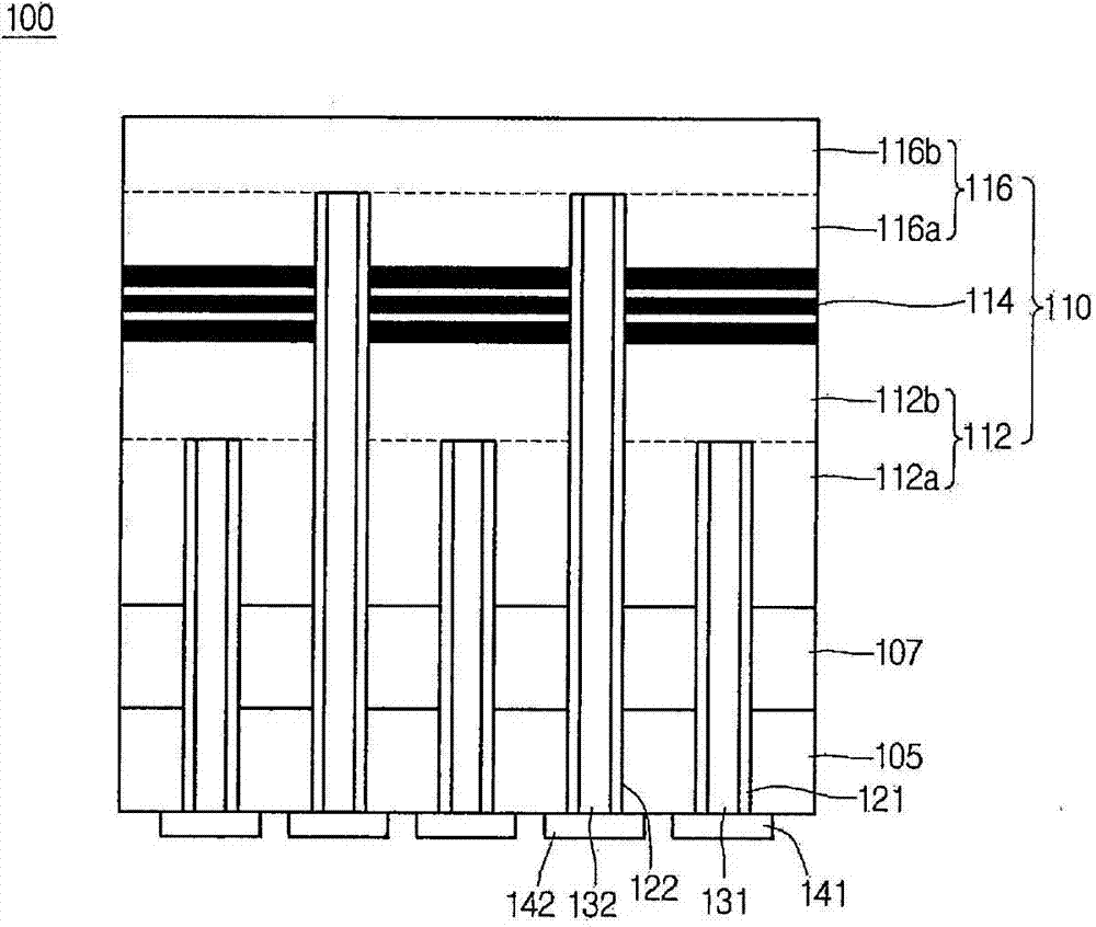
[0025] figure 1 To illustrate a cross-sectional view of the light emitting device 100 according to the first embodiment.

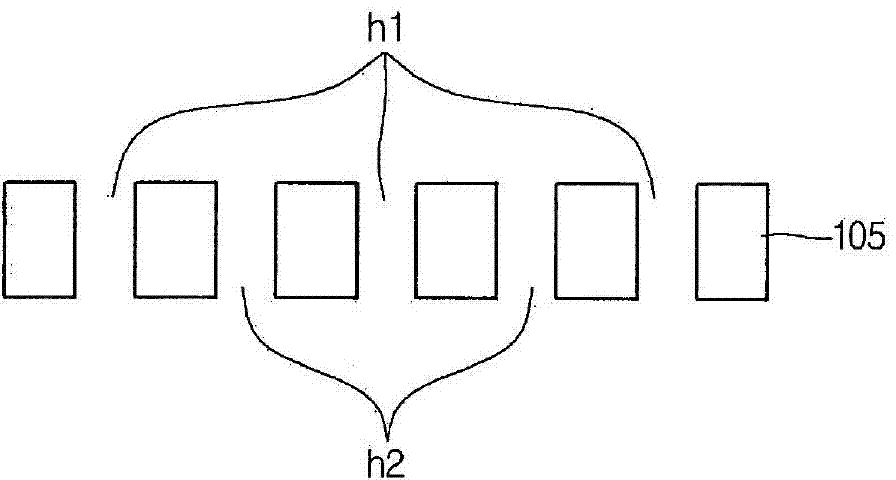
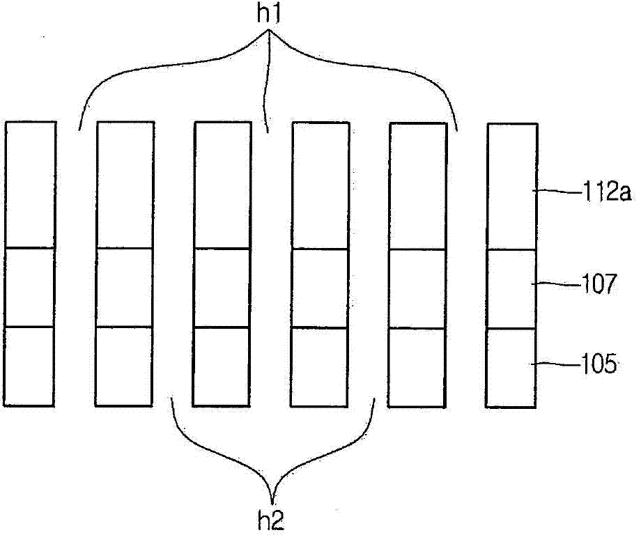
[0026] The light emitting device 100 according to the first embodiment may include: a substrate 105; a first conductive semiconductor layer 112 on the substrate 105; an active layer 114 on the first conductive semiconductor layer 112; a second conductive semiconductor layer on the active layer. Two conductive semiconductor layers 116; a first via electrode 131, the first via electrode 131 is in contact with the first conductive semiconductor layer 112 through a through hole h1 formed through the substrate 105; and a second via electrode 132, the The second via electrode 132 contacts the second conductive semiconductor layer 116 through the second via hole h2 formed through the substrate 105 , the first conductive semiconductor layer 112 and the active layer 114 .

[0027] The first conductive semiconductor layer 112 , the active layer 114 and the second c...


PUM


Abstract

Disclosed are a light emitting device, a method of manufacturing the same, a light emitting device package, and a lighting system. The light emitting device includes a substrate, a first conductive semiconductor layer on the substrate, an active layer on the first conductive semiconductor layer, a second conductive semiconductor layer on the active layer, a first via electrode to make contact with the first conductive semiconductor layer through a via hole formed through the substrate, and a second via electrode to make contact with the second conductive semiconductor layer through a second via hole formed through the substrate, the first conductive semiconductor layer, and the active layer.

Description

technical field [0001] The present embodiment relates to a light emitting device, a method of manufacturing a light emitting device, a light emitting device package, and a lighting system. Background technique [0002] A light emitting device (LED) includes a PN junction diode having a characteristic of converting electrical energy into light energy. A PN junction diode can be produced by using a compound semiconductor including group III-V elements in the periodic table. By adjusting the composition ratio of compound semiconductors, light emitting devices can exhibit various colors. [0003] LEDs according to the related art may be classified into lateral type LEDs and vertical type LEDs according to positions of electrode layers. [0004] Meanwhile, according to the LED packaging technology of the related art, the flip chip LED is based on a lateral type LED, and a hole injection semiconductor layer and an active layer are etched to form an N-type electrode. Therefore, ...

Claims


Application Information

Patent Timeline
Patent Type & Authority Applications(China)
IPC IPC(8): H01L33/38H01L33/40H01L33/62F21S2/00F21Y101/02
CPCH01L33/382H01L2924/0002H01L2924/00H01L33/36H01L33/38H01L33/62
Inventor 林东旭
Owner SUZHOU LEKIN SEMICON CO LTD
Learn More