Etching device reaction chamber electrode and etching device

A technology for etching equipment and reaction chambers, applied in circuits, discharge tubes, electrical components, etc., can solve the problem of cumbersome removal of electrode holes, save time for electrode maintenance, improve performance, and be easy to maintain.

Inactive Publication Date: 2014-05-07
BEIJING BOE OPTOELECTRONCIS TECH CO LTD +1
View PDF5 Cites 5 Cited by
  • Summary
  • Abstract
  • Description
  • Claims
  • Application Information

AI Technical Summary

Problems solved by technology

[0006] The technical problems to be solved by the present invention include, aiming at the problem that the electrode needs to be dismantled as a whole when the electrode hole of the existing dry etching equipment is blocked and the disassembly is extremely cumbersome. Corrosion equipment, which can repair the blocked electrode hole without dismantling the electrode as a whole

Method used


Image

  • Etching device reaction chamber electrode and etching device
  • Etching device reaction chamber electrode and etching device
  • Etching device reaction chamber electrode and etching device

Examples


Embodiment Construction

[0026] In order to enable those skilled in the art to better understand the technical solutions of the present invention, the present invention will be further described in detail below in conjunction with the accompanying drawings and specific embodiments.

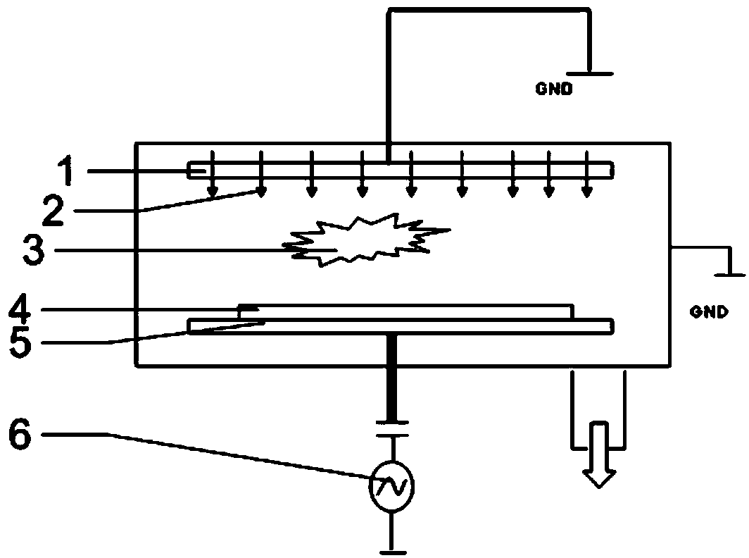
[0027] An embodiment of the present invention provides an electrode of a reaction chamber of an etching device. The etching device is preferably a dry etching device, and the electrode is preferably an upper electrode of the reaction chamber of the dry etching device. The dry etching equipment can be used to etch the film layer deposited on the substrate during the manufacturing process of liquid crystal display, organic light emitting diode display and the like.

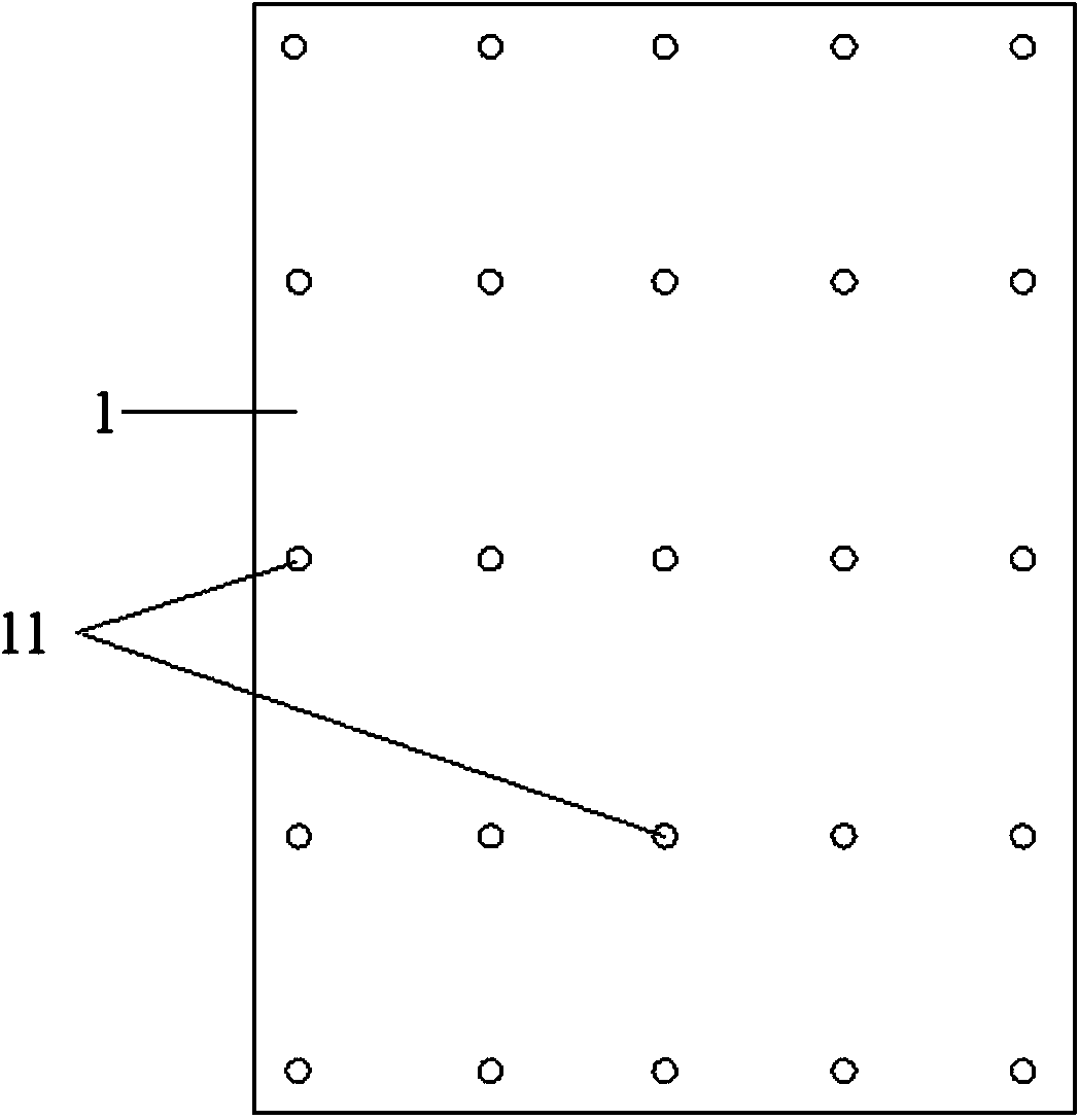
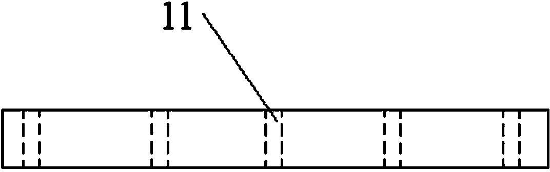
[0028] Such as Figure 4 to Figure 6 As shown, the electrode of this embodiment includes a flat plate 8, and the flat plate 8 is provided with a plurality of first through holes 12, and the electrode also includes a plurality of inserts 7 with second through ho...


PUM


Abstract

The invention provides an etching device reaction chamber electrode and an etching device, and pertains to the technical field of display device manufacture. When electrode holes of an existing dry etching device are blocked, the whole electrode needs to be disassembled and the disassembly process is complex; according to the invention, the problem can be solved. The etching device reaction chamber electrode of the invention comprises a flat plate. The flat plate is provided with a plurality of first through holes. The electrode further comprises a plurality of embedment elements provided with second through holes. The embedment elements are embedded into the first through holes. The etching device of the invention comprises the above etching device reaction chamber electrode. According to the invention, the maintenance of the etching device reaction chamber electrode is more time-saving and labor-saving.

Description

technical field [0001] The invention belongs to the technical field of display device manufacturing, and in particular relates to an etching equipment [0002] Electrodes and etching equipment for the reaction chamber. Background technique [0003] In the manufacturing process of Thin Film Transistor-Liquid Crystal Display (TFT-LCD for short), etching is one of the important processes, and etching is divided into dry etching and wet etching. Such as figure 1 As shown, the dry etching uses a radio frequency power supply 6 to excite the reactive gas 2 to generate a low-temperature plasma 3, and generates ions and free radicals during the reaction, and the ions and free radicals react with the material deposited on the substrate 4 that is not covered by the photoresist Volatile species are generated to transfer the pattern specified by the mask to the substrate. [0004] For existing dry etching equipment, such as figure 2 and image 3 As shown, the reaction chamber inclu...

Claims


Application Information

Patent Timeline
Patent Type & Authority Applications(China)
IPC IPC(8): H01J37/32H01L21/67
Inventor 蒋会刚肖红玺谢海征高建剑高福亮蒋晓纬
Owner BEIJING BOE OPTOELECTRONCIS TECH CO LTD
Why Eureka
Try Eureka