Multilayered printed circuit board plated-through hole stress-strain model establishing method based on girder construction

A printed circuit board and model building technology, which is applied in the fields of printed circuit components, electrical connection formation of printed components, electrical digital data processing, etc., can solve the problem of not satisfying the boundary free condition and displacement continuous condition, and the model does not include the number of board layers , does not meet the boundary conditions and other problems, to achieve the effect of good engineering application prospects

Active Publication Date: 2014-05-07
BEIHANG UNIV
View PDF3 Cites 5 Cited by
  • Summary
  • Abstract
  • Description
  • Claims
  • Application Information

AI Technical Summary

Problems solved by technology

The IPC model simplifies the plated through hole to a one-dimensional rod structure, which is simple and easy to calculate, but does not satisfy the boundary free condition and displacement continuous condition
The stress distribution model of plated through holes takes into account the shear force at the copper-resin interface, which makes the estimation results more in line with the actual situation, but the model does not include the influence of the number of board layers and pads
The CALCE model compares plated through holes to series-parallel springs, taking multilayer boards and pads into account, but does not satisfy boundary conditions
The Mirman model simplifies the pad to a beam structure, considering the influence of the external pad, but does not give the force in the pad

Method used


Image

  • Multilayered printed circuit board plated-through hole stress-strain model establishing method based on girder construction
  • Multilayered printed circuit board plated-through hole stress-strain model establishing method based on girder construction
  • Multilayered printed circuit board plated-through hole stress-strain model establishing method based on girder construction

Examples


Embodiment Construction

[0060] A method for establishing a stress-strain model of a plated through hole of a multilayer printed circuit board based on a beam structure according to the present invention, the process flow of which is shown in image 3 As shown, the specific implementation steps of the method are as follows:

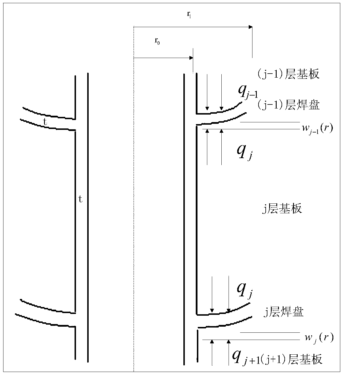
[0061] There are many parameters involved in the specific implementation steps, and the symbols and meanings of the parameters are summarized as follows:

[0062] r is the position coordinate along the radial direction of the plated through hole; r 0 is the hole radius; r 1 is the pad radius; w j is the pad deflection of layer j; D j is pad stiffness of layer j; q j is the substrate load between (j-1) and j-layer pads; q j+1 is the substrate load between j and (j+1) layer pads; A, B, C and D are the introduced undetermined coefficients; E Cu is the modulus of elasticity of the copper material; E Cu ’ is the plastic modulus of the coating material within the plastic range; ...


PUM


Abstract

The invention provides a multilayered printed circuit board plated-through hole stress-strain model establishing method based on girder construction. The multilayered printed circuit board type plated-through-hole stress-strain model establishing method based on the girder construction comprises the following steps: 1, simplifying a multilayered printed circuit board plated-through-hole to be the girder construction in axial symmetry, and establishing assumed conditions based on the girder construction; 2, regarding a bonding plate structure as an annular round plate to be uniformly loaded, and setting boundary conditions of inner-diameter simply support and external-diameter free of a bonding plate; 3, writing mechanical ordinary differential equations of the bonding plate based on assumption that the bonding plate is uniformly loaded, and solving a general solution expression of a deflection; 4, determining four coefficients to be determined in the general solution expression by using the boundary conditions, and listing relationship of the load, and the deflection, a bearing force and a thermal strain by combining displacement continuous conditions; 5, determining radial, annular and axial stresses at the position with the maximum stress by combining the boundary conditions and calculating an equivalent stress by using a Mises equivalent stress computational formula; 6, giving a strain analysis expression within a range of elasticity and plasticity of a multilayered printed circuit board plated-through hole according to linear elasticity and linear plasticity stress-strain relationship of a coating material.

Description

Technical field: [0001] The invention relates to a method for establishing a stress-strain model of a plated through hole of a multilayer printed circuit board based on a beam structure. Through the analysis of the stress-strain distribution of the through hole, the stress-strain analytical model of the plated through hole of the multilayer printed circuit board is obtained. This method belongs to the field of failure physical model modeling of electronic products. Background technique: [0002] Printed circuit boards are an indispensable part of electronic equipment. In order to reduce the interconnection lines between electronic components, multilayer packaging structures have been widely used. Used to provide electrical connections for different board layers, plated through holes have become a key component of printed circuit boards, and the reliability of plated through holes has become a key factor in the reliability of printed circuit boards. [0003] PTH reliability ...

Claims


Application Information

Patent Timeline
IPC IPC(8): G06F17/50H05K1/11H05K3/42
Inventor 胡薇薇刘晨艳孙宇锋赵广燕
Owner BEIHANG UNIV
Why Eureka
Try Eureka