


Quick Research
Generate reliable direction feasibility study reports for your R&D in just a few steps.

Technical Q&A
Discover and master advanced knowledge NOW. Basics, ideas, possibilities, all at once.

Find Solutions
As an expert in R&D theories, this can generate solutions to your technical problems instantly.

Evaluate Feasibility
Analyze your overall solution with one click, know your potential R&D risks in advance.

Monitor Landscape
Get weekly tech updates, stay abreast of the latest tech innovations and key insights.
Synthetic method of high-selectivity comb-type CdS nanometer material
A nanomaterial, high-selectivity technology, applied in the fields of nanotechnology, nanotechnology, nanotechnology for materials and surface science, etc., can solve the problems of rare reports of high-selectivity comb CdS nanomaterials, and achieve good repeatability. sexual effect
- Summary
- Abstract
- Description
- Claims
- Application Information
AI Technical Summary
Problems solved by technology
Method used
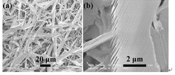
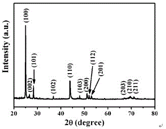
Image

Examples
Embodiment Construction
[0012] Below are examples of the present invention (reagents used in the examples are all chemically pure), the main steps of the experimental process:
[0013] First, use a small ion sputtering device to coat a layer of Au film with a thickness of about 50 nm on a (100) crystal orientation Si substrate with a size of 0.9 cm*0.9 cm; put a ceramic boat containing 1.4 g of CdS powder into a quartz tube And push it to the position of the thermocouple of the tube furnace, push the Si substrate coated with Au film into the quartz tube to a position 17 cm away from the left side of the ceramic boat, seal the quartz tube, use a mechanical pump to pump air for 1 h, and then move it from the right Argon gas was introduced into the side at a flow rate of 30 sccm, and the gas flow rate of the gas inlet and outlet on both sides of the enamel was adjusted, and the air pressure in the quartz tube was maintained at 0.1 MPa by using a mechanical pump; under the protection of argon gas, the rea...
PUM
| Property | Measurement | Unit |
|---|---|---|
| thickness | aaaaa | aaaaa |
Abstract
Description
Claims
Application Information
 - R&D Engineer
- R&D Manager
- IP Professional
- Industry Leading Data Capabilities
- Powerful AI technology
- Patent DNA Extraction
Browse by: Latest US Patents, China's latest patents, Technical Efficacy Thesaurus, Application Domain, Technology Topic, Popular Technical Reports.
© 2024 PatSnap. All rights reserved.Legal|Privacy policy|Modern Slavery Act Transparency Statement|Sitemap|About US| Contact US: help@patsnap.com