
Eight-shaft-moving chip repairing and attaching device and method with visual positioning function

A technology of visual positioning and placement devices, which is applied in the direction of assembling printed circuits with electrical components, can solve problems that are not conducive to improving the quality of desoldering and placement, unfavorable work efficiency, labor costs, automatic adjustment of heating height, etc., to achieve saving Labor cost, wide application range, and the effect of improving work efficiency

Inactive Publication Date: 2014-04-09
古国柱
View PDF4 Cites 12 Cited by
  • Summary
  • Abstract
  • Description
  • Claims
  • Application Information

AI Technical Summary

Problems solved by technology

Existing rework workstations usually have poor flexibility, and can only operate one PCB board at a time, so the work efficiency is low, which is not conducive to improving work efficiency and saving labor costs; and after completing the desoldering or welding of a PCB board After that, it cannot automatically carry out the operation of the next PCB board, and frequent manual refueling is required, which is not conducive to improving work efficiency
In addition, the existing rework station heating device cannot automatically adjust the heating height according to the different chips, so its heating performance is poor, which is not conducive to improving the quality of desoldering and placement

Method used


Image

  • Eight-shaft-moving chip repairing and attaching device and method with visual positioning function
  • Eight-shaft-moving chip repairing and attaching device and method with visual positioning function
  • Eight-shaft-moving chip repairing and attaching device and method with visual positioning function

Examples


Embodiment Construction

[0048] The following examples are further explanations and supplements to the present invention, and do not constitute any limitation to the present invention.

[0049] The eight-axis mobile chip rework and chip placement device with visual positioning of the present invention is equipped with eight linear moving guide rail pairs, which have moving tracks in eight directions, so it has high flexibility and can be used for a variety of chips packaged in BGA Desoldering and SMT operations, and can greatly improve work efficiency.

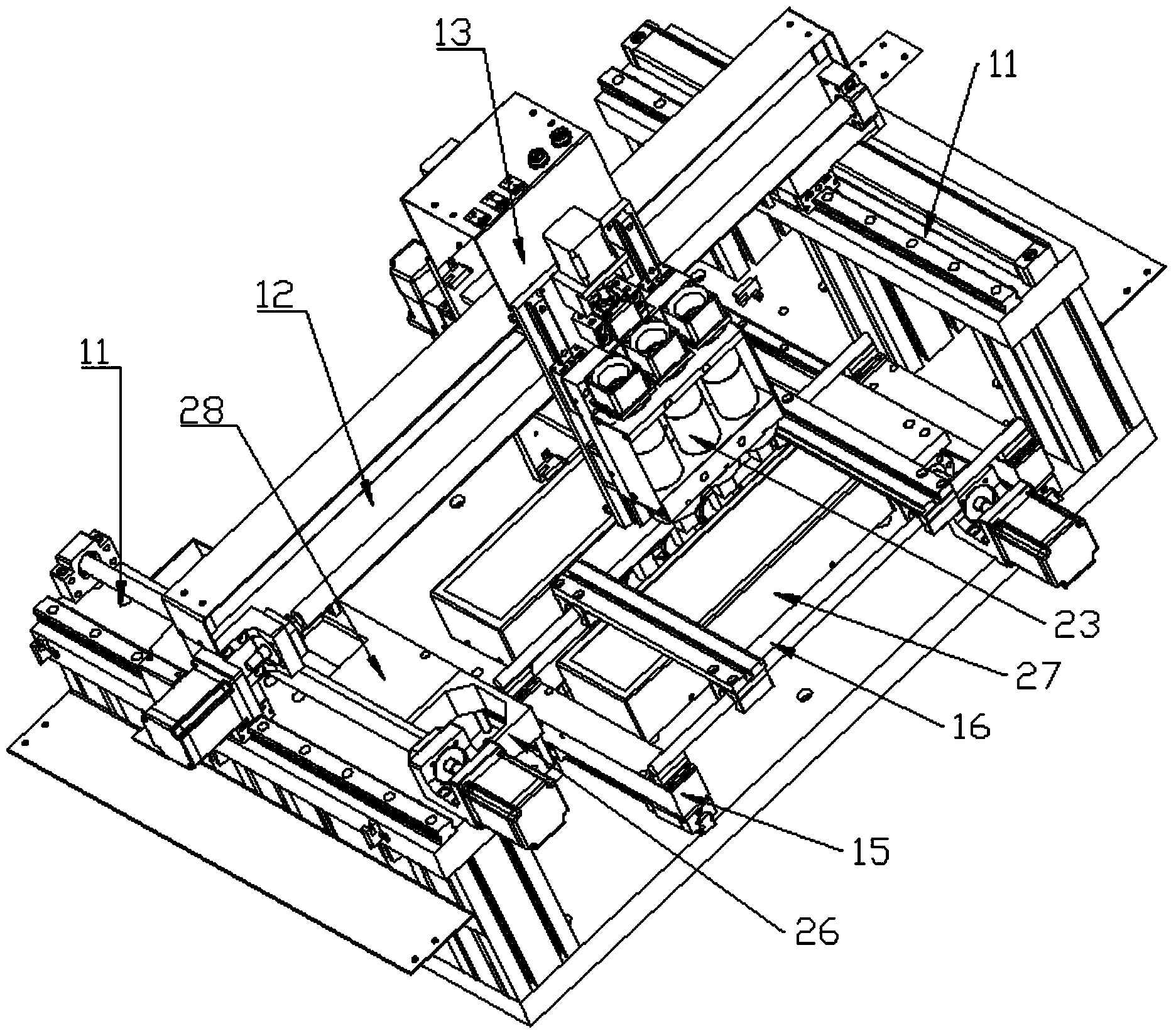
[0050] Specifically, as Figure 1 to Figure 13 As shown, the eight linear guide rail pairs include the first linear guide rail pair 11, the second linear guide rail pair 12, the third linear guide rail pair 13, the fourth linear guide rail pair 14, the fifth linear guide rail pair 15, the sixth linear guide rail pair The linear guide rail pair 16 , the seventh linear guide rail pair 17 and the eighth linear guide rail pair 18 .

[0051] Such as Fi...


PUM


Abstract

The invention discloses an eight-shaft-moving chip repairing and attaching device and method with a visual positioning function. The device is provided with a first linear guide rail pair, a second linear guide rail pair, a third linear guide rail pair, a fourth linear guide rail pair, a fifth linear guide rail pair, a sixth linear guide rail pair, a seventh linear guide rail pair, an eighth linear guide rail pair, a tray assembly, a first heating assembly, a second blowing assembly, a third heating assembly, a first visual positioning assembly, a second visual positioning assembly and a chip taking and attaching assembly. Multi-dimensional motion trails are provided by the several linear guide rail pairs so that the tray assembly, the heating assemblies, the visual positioning assemblies and the chip taking and attaching assembly can be controlled by a controller to achieve positioning, heating, taking and placing flexibly, and therefore the sealing-off and chip attaching function can be achieved. Because the several linear guide rail pairs and the heating assemblies are arranged, a plurality of PCBs or chips can be operated at the same time, and accordingly the sealing-off and chip attaching efficiency can be greatly improved, and human cost can be greatly reduced as well.

Description

【Technical field】 [0001] The invention relates to chip rework and soldering, in particular to an eight-axis moving chip rework and patch device with visual positioning that can provide work efficiency and a method thereof. 【Background technique】 [0002] BGA package, that is, solder ball array package, is to make an array of solder balls on the bottom of the package substrate as the I / O terminal of the circuit to interconnect with the printed circuit board (PCB board). When a BGA-packaged chip fails and needs to be reworked, the rework station is usually used for the operation. The existing rework process is usually as follows: 1. Remove the chip from the PCB board - melt the solder by heating, and use a vacuum nozzle to suck up the chip; 2. Implant solder balls on the back of the chip substrate - remove the solder on the substrate. Tin slag, evenly coated with flux, then put into the corresponding stencil fixture, pour the solder ball into the stencil, so that each solder ...

Claims


Application Information

Patent Timeline
IPC IPC(8): H05K3/34
Inventor 古国柱周君丽
Owner 古国柱
Learn More