
A Resistive Variable Memory Capable of Realizing Multi-value Storage

A technology of resistive variable memory and multi-value storage, which is applied in the direction of electrical components, etc.

Active Publication Date: 2018-11-09
SHANGHAI INTEGRATED CIRCUIT RES & DEV CENT
View PDF10 Cites 0 Cited by
  • Summary
  • Abstract
  • Description
  • Claims
  • Application Information

AI Technical Summary

Problems solved by technology

However, with the continuous development of microelectronic technology process nodes, Flash memories based on traditional floating gate structures are facing severe challenges in data storage reliability.

Method used


Image

  • A Resistive Variable Memory Capable of Realizing Multi-value Storage
  • A Resistive Variable Memory Capable of Realizing Multi-value Storage

Examples


Embodiment Construction

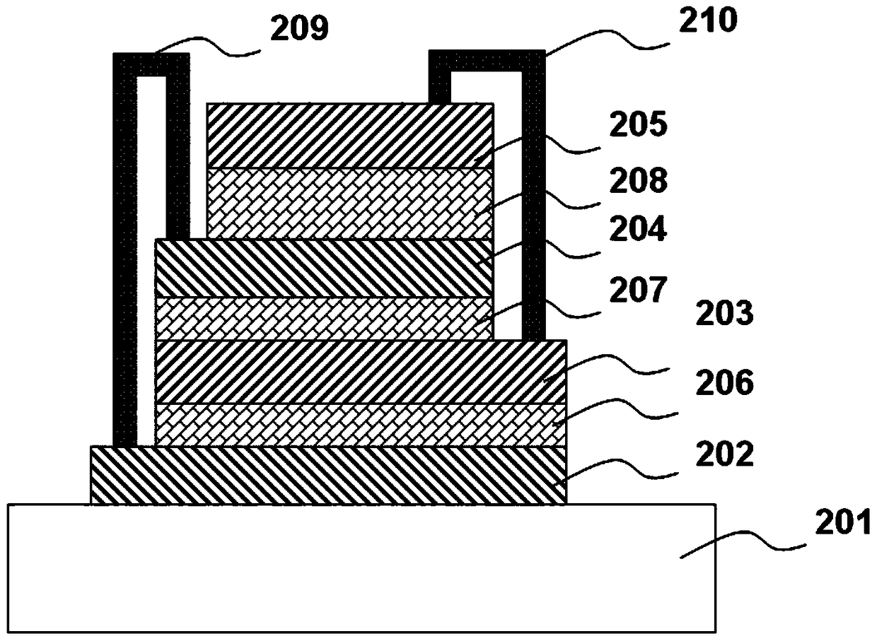
[0021] Attached below figure 2 , the specific embodiment of the present invention will be further described in detail.

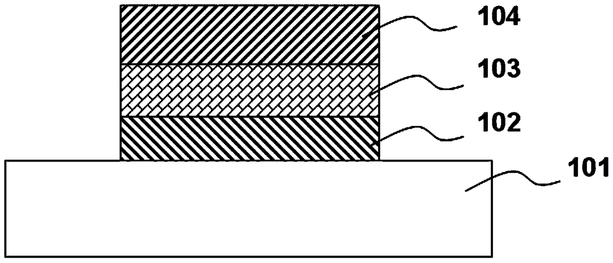
[0022] It should be noted that the present invention has a resistive variable memory with a stacked structure, including a semiconductor substrate, an N-1 group double-layer structure, and a top electrode located on the N-1 group double-layer structure; Each group of double-layer structures is composed of an electrode and a resistive layer on the electrode. The N-1 group of double-layer structures is located on the substrate and stacked sequentially from bottom to top, where N is a positive integer greater than or equal to 3 ; Wherein, all odd-numbered electrodes from bottom to top are connected in parallel as the lower electrodes of the RRAM, and all even-numbered electrodes from bottom to top are connected in parallel as upper electrodes of the RRAM. Taking N as 4 as an example below, the present invention will be further described in detail.

[0023] s...


PUM


Abstract

The invention discloses a resistive random access memory capable of realizing multilevel storage. The resistive random access memory capable of realizing the multilevel storage comprises a semiconductor substrate, N-1 groups of double-layer structures and top electrodes on the N-1 groups of double-layer structures, wherein each N-1 group of double-layer structure consists of an electrode and one resistive layer positioned on the electrode; the N-1 groups of double-layer structures are positioned on the substrate and are successively overlaid from bottom to top, wherein N is a positive integer greater than or equal to 3; all odd-number electrodes from bottom to top are connected in parallel to serve as the lower electrode of the resistive random access memory; all even-number electrodes from bottom to top are connected in parallel to serve as the upper electrode of the resistive random access memory. Therefore, according to the resistive random access memory capable of realizing the multilevel storage, which is disclosed by the invention, in a mode that multiple electrodes and the resistive layers are alternatively overlaid, voltages required for each resistive layer to generate resistance change are different, resistance values after the resistance change happens are different, so that the multilevel storage of a memory unit structure is realized, and no additional area is occupied by the memory unit disclosed by the invention because of adopting a longitudinal-overlaying structure.

Description

technical field [0001] The invention belongs to the field of non-volatile semiconductor memory, and in particular relates to a resistive variable memory for multi-value storage. Background technique [0002] In the electronic information age, semiconductor memory plays a vital role in information storage. Non-volatile memory has a greater advantage in mobile storage media because data can still be retained after power failure. A typical device structure of the current non-volatile memory is a floating gate type memory. However, with the continuous development of microelectronic technology process nodes, the Flash memory based on the traditional floating gate structure is facing severe challenges of data storage reliability. [0003] In order to deal with the problems encountered by traditional floating gate Flash, various new types of non-volatile memory have been developed rapidly in recent years, mainly including discrete charge memory (such as nanocrystalline and SONOS)...

Claims


Application Information

Patent Timeline
Patent Type & Authority Patents(China)
IPC IPC(8): H01L45/00
Inventor 范春晖左青云周伟
Owner SHANGHAI INTEGRATED CIRCUIT RES & DEV CENT
Learn More