Wafer Defect Inspection Method

A defect detection and wafer technology, applied in semiconductor/solid-state device testing/measurement, electrical components, circuits, etc., can solve problems such as reducing defect detection accuracy, reducing process efficiency, increasing process steps, etc., to improve defect recognition rate, Improve adaptability and facilitate the effect of promotion

Active Publication Date: 2016-10-12
SHANGHAI HUALI MICROELECTRONICS CORP
View PDF3 Cites 0 Cited by
  • Summary
  • Abstract
  • Description
  • Claims
  • Application Information

AI Technical Summary

Problems solved by technology

[0004] In the current wafer preparation process, the size of the wafer is constantly increasing, from 200mm to 300mm or even 450mm today, and the process parameters such as film thickness and circuit size of each chip area on the wafer will also vary greatly. Figure 2A It shows the film thickness distribution of each chip area of ​​the wafer after chemical mechanical polishing. The film thickness value can be divided into 4 intervals: 340-350nm, 350-360nm, 360-370nm and 370-380nm. For different film thicknesses on the wafer For these four areas, if the same detection light source (constant wavelength) is used to scan the defects of the four chip areas whose film thicknesses are in the above four intervals, the following can be obtained: Figure 2B As shown in the image, it can be seen that due to the difference in film thickness of each chip area, the same physical structure exhibits different grayscale characteristics under the same inspection light source. However, the current defect inspection methods usually use inspection parameters that cannot be adaptive. As a result, a lot of noise signals may be generated during defect detection, and even non-defect areas are detected as defect areas, which not only reduces the accuracy of defect detection, but also may lead to unnecessary process steps, thereby reducing process efficiency

Method used


Image

  • Wafer Defect Inspection Method
  • Wafer Defect Inspection Method
  • Wafer Defect Inspection Method

Examples


Embodiment Construction

[0016] The specific embodiment of the present invention will be further described in detail below in conjunction with the accompanying drawings.

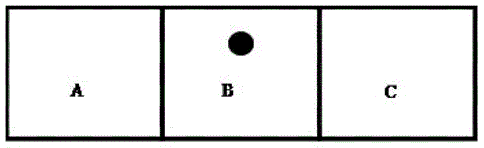
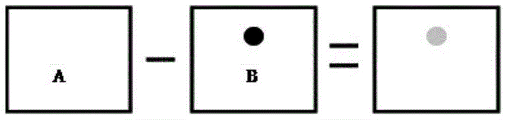
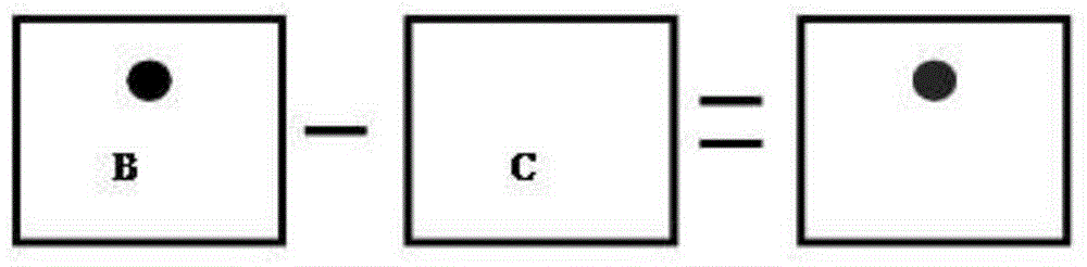
[0017] It should be noted that the wafer includes a plurality of chip areas, and the chips are separated by dicing lines. The detection of wafer defects is essentially the detection of defects on each chip. In the embodiment provided by the present invention, the detection of wafer defects by the detection beam is used in combination with an industrial camera. The area on the wafer on which the detection beam is projected is observed by the industrial camera, and combined with certain image processing measures, the image gray The identification and comparison of high-degree features can effectively detect defects on the wafer.

[0018] Such as image 3 As shown, the wafer defect detection method provided by an embodiment of the present invention includes the following process steps:

[0019] Step S10 , detecting the film thickness...


PUM


Abstract

The invention relates to a wafer defect detection method which comprises the following steps: detecting film thickness of each chip area on a wafer; dividing the surface of the wafer into a plurality of detection areas according to film thickness distribution information of each chip area, wherein each detection area includes at least one chip area; selecting a detection light beam of a determined wavelength for each detection area to enable gray features of the structurally-identical chip areas under projection of the detection light beams to be similar; and successively projecting each detection light beam in each chip area of the detection area corresponding to the detection light beam and detecting the defect of the chip area according to the gray features of the chip area. The method improves the adaptability of the wafer with non-uniform film thickness distribution, significantly improves the defect identification rate and is high in precision, low in cost and easy to promote in the field.

Description

technical field [0001] The invention relates to the technical field of semiconductor processing and manufacturing, and more specifically, to a wafer defect detection method. Background technique [0002] The advanced integrated circuit manufacturing process generally includes hundreds of steps, and a small error in any link will lead to the failure of the entire chip, especially as the critical size of the circuit continues to shrink, the requirements for process control become stricter, so In the production process, in order to find and solve problems in time, optical and electronic defect detection equipment are equipped to carry out online detection of products. [0003] The basic principle of optical and electronic defect detection is to collect the signals of several chips through the equipment, and convert the physical image on the chip into a data image that can be represented by different bright and dark gray scales. A method for detecting defects on a wafer in the ...

Claims


Application Information

Patent Timeline
Patent Type & Authority Patents(China)
IPC IPC(8): H01L21/66
CPCH01L22/12H01L22/24
Inventor 倪棋梁陈宏璘龙吟
Owner SHANGHAI HUALI MICROELECTRONICS CORP
Why Eureka
Try Eureka