Method for improving photoetching process used on Al2O3 medium
A lithography process and medium technology, which is applied in the direction of photosensitive material processing, micro-lithography exposure equipment, photolithography process exposure device, etc., can solve the problems affecting device performance, small process tolerance, easy to be corroded, etc., and achieve device performance Stable, small process tolerance, avoid corrosion effect
- Summary
- Abstract
- Description
- Claims
- Application Information
AI Technical Summary
Problems solved by technology
Method used
Image


Examples
Embodiment 1
[0028] Example 1: Al photoetched based on AZ4620 photoresist 2 o 3 Medium layer, the specific steps are as follows:
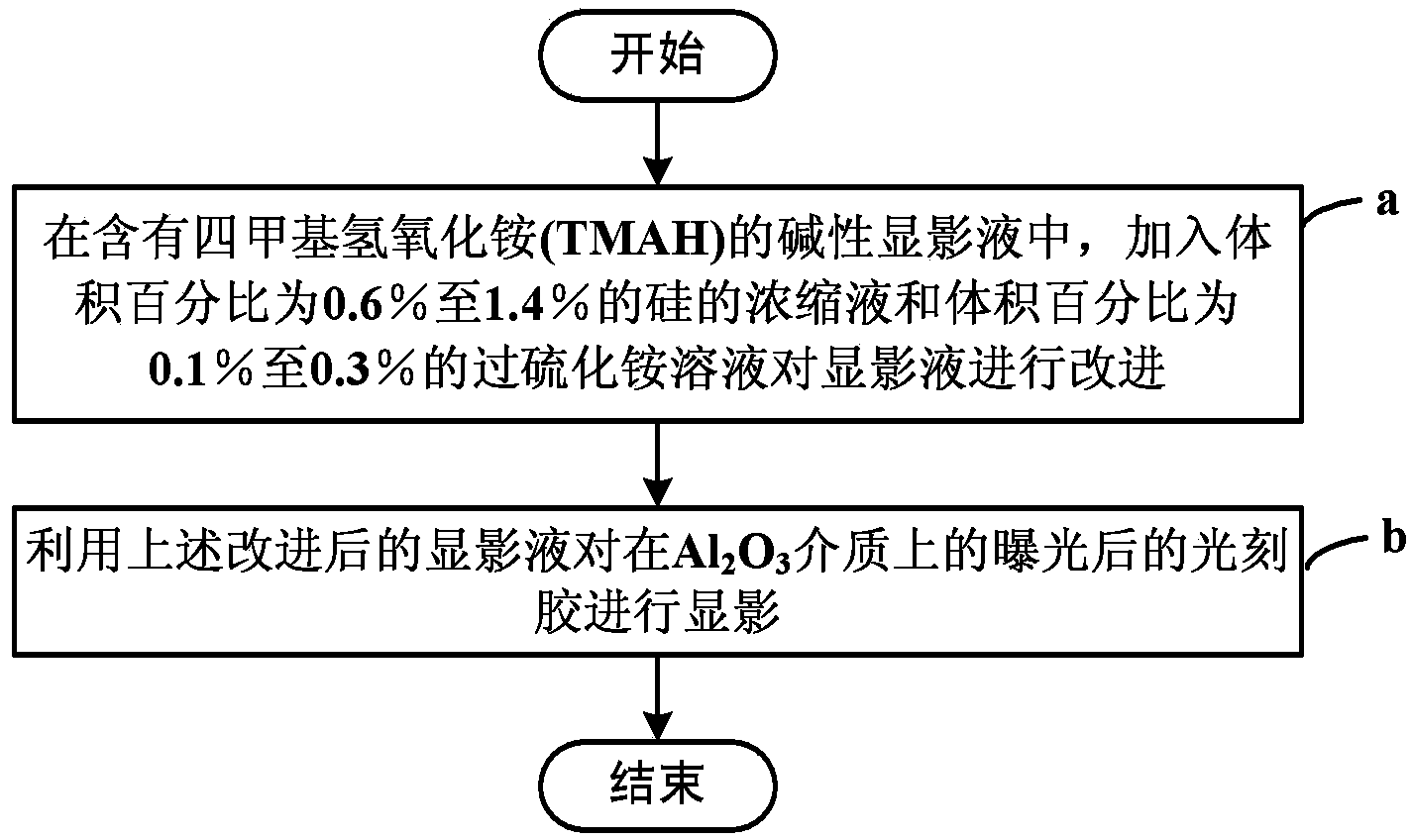
[0029] Step 1: In an alkaline developing solution containing tetramethylammonium hydroxide, add a concentrated solution of silicon (Si) with a volume percentage of about 1% and ammonium persulfide ((NH) with a volume percentage of about 0.2% 4 ) 2 S 2 o 8 ) solution;
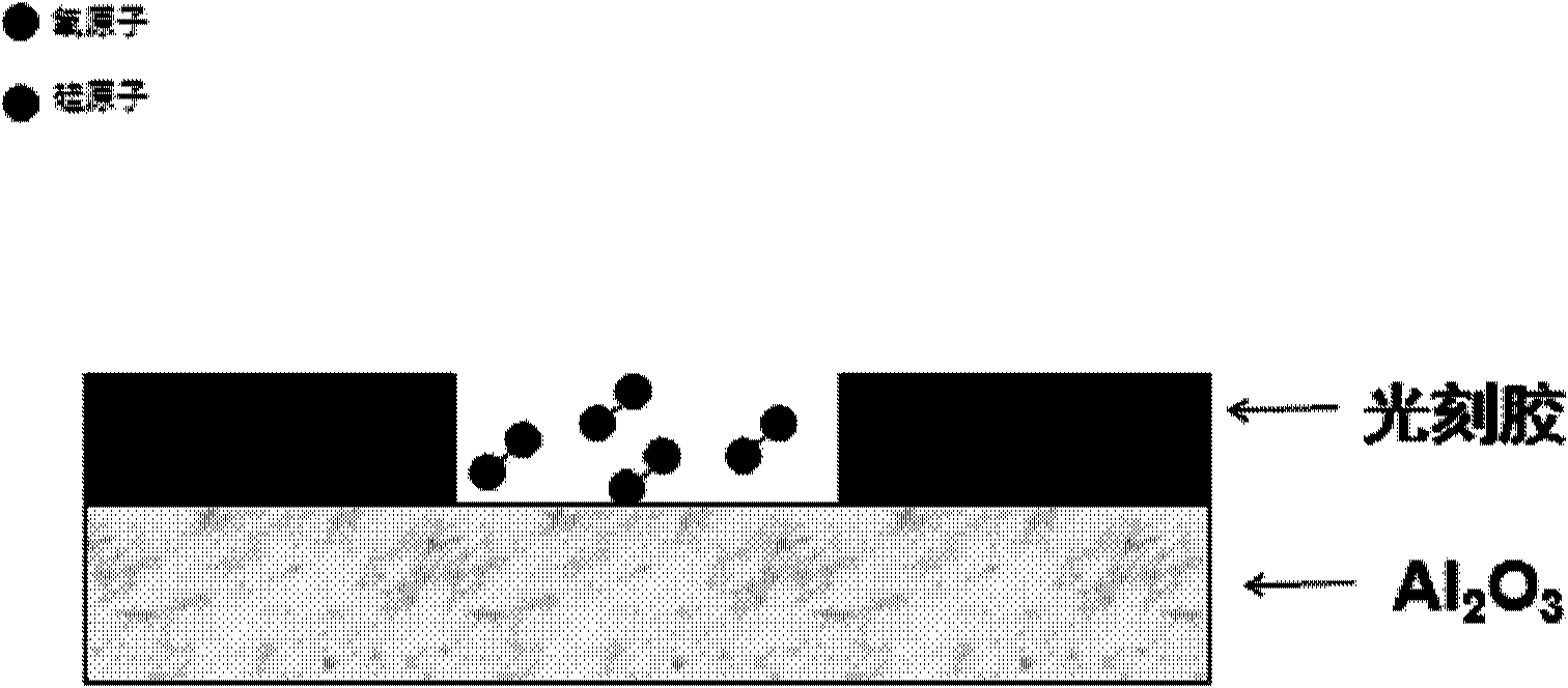
[0030] Step 2: Use the above-mentioned improved developer solution on Al 2 o 3 The exposed photoresist on the media is developed.
Embodiment 2
[0031] Embodiment 2: Al photoetched based on AZ5214 photoresist 2 o 3 medium layer, the specific steps are as follows.
[0032] Step 1: In the alkaline developer solution containing tetramethylammonium hydroxide, add the concentrated solution of silicon (Si) with a volume percentage of about 1% and ammonium persulfide ((NH) with a volume percentage of about 0.2% 4 ) 2 S 2 o 8 ) solution;
[0033] Step 2: Use the above-mentioned improved developer solution on Al 2 o 3 The exposed photoresist on the media is developed.
Embodiment 3
[0034] Embodiment 3: Al photoetched based on AZ6112 photoresist2 o 3 Medium layer, the specific steps are as follows:
[0035] Step 1: In the alkaline developer solution containing tetramethylammonium hydroxide, add the concentrated solution of silicon (Si) with a volume percentage of about 1% and ammonium persulfide ((NH) with a volume percentage of about 0.2% 4 ) 2 S 2 o 8 ) solution;
[0036] Step 2: Use the above-mentioned improved developer solution on Al 2 o 3 The exposed photoresist on the media is developed.
PUM
 Abstract
Description
Claims
Application Information
 - R&D
- Intellectual Property
- Life Sciences
- Materials
- Tech Scout
- Unparalleled Data Quality
- Higher Quality Content
- 60% Fewer Hallucinations
Browse by: Latest US Patents, China's latest patents, Technical Efficacy Thesaurus, Application Domain, Technology Topic, Popular Technical Reports.
© 2025 PatSnap. All rights reserved.Legal|Privacy policy|Modern Slavery Act Transparency Statement|Sitemap|About US| Contact US: help@patsnap.com