Surface nanotechnology locally-processed thin-wall energy absorption tube
A nanotechnology and energy-absorbing tube technology, applied in the field of thin-walled energy-absorbing tubes, can solve the problems that surface nanotechnology has not yet applied energy-absorbing structures and devices, and achieve the effects of low load uniformity coefficient, simple structure, and easy processing.
- Summary
- Abstract
- Description
- Claims
- Application Information
AI Technical Summary
Problems solved by technology
Method used
Image
Examples
Embodiment 1
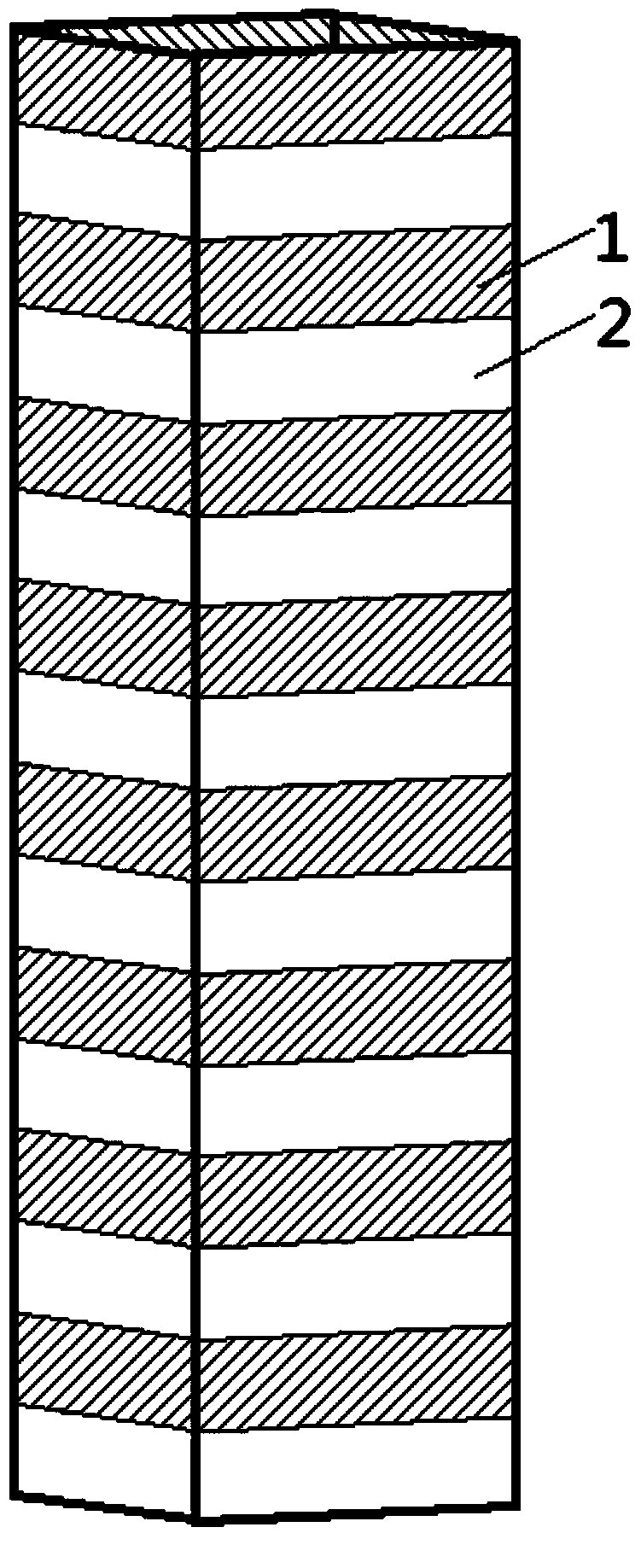
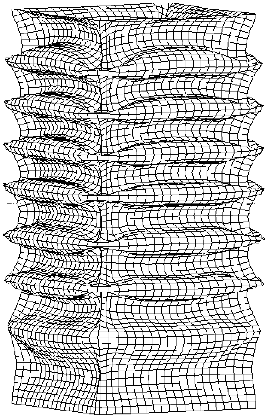
[0030] Example 1: The dimensions of a thin-walled energy-absorbing tube with a square cross-section are: the side length of the section is 40 mm, the tube length is 160 mm, the wall thickness is 0.5 mm, and the twin spacing of the surface nanometerization index is 35 nm. figure 1 A thin-walled energy-absorbing tube with a square cross-section that is locally treated with nanotechnology on the circumferentially equidistantly spaced strip-shaped surface. The lower end is fixed, and the upper end is axially punched by a 90kg mass block. "1" on the local surface of the thin-walled energy-absorbing tube indicates the nano-scaled area on the surface, and the four surfaces are treated with the same nano-scale, and the best 8 such strips are used on each surface, and the positions are the same, such as figure 1 shown. The size of the circumferential spacer strip is 40mm long and 10mm wide. Under the axial punching of the mass block at a speed of 6m / s, the thin-walled energy-absorbin...
Embodiment 2
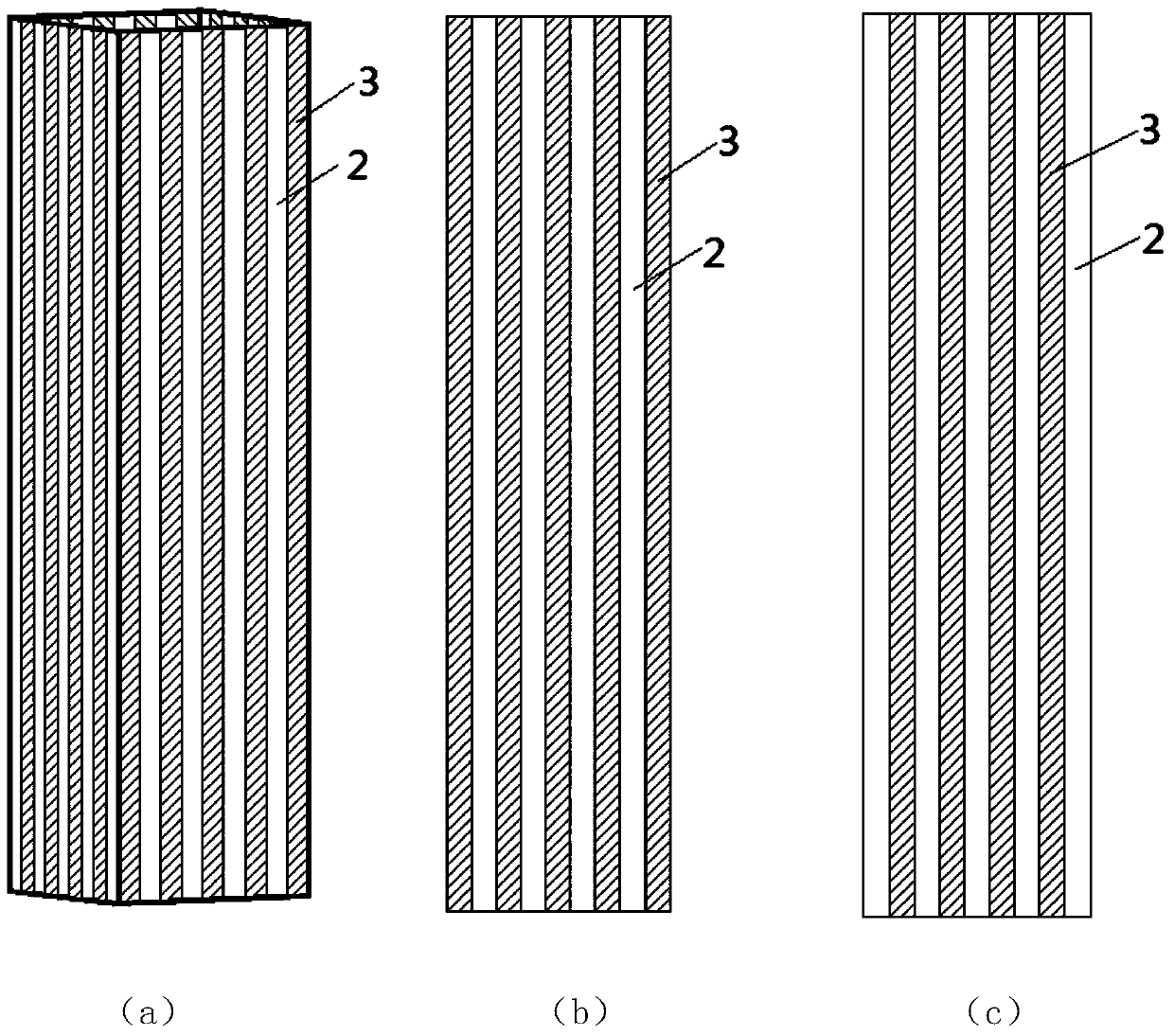
[0031] Embodiment 2: The dimensions of a thin-walled energy-absorbing tube with a square cross section are: the side length of the section is 40 mm, the tube length is 160 mm, the wall thickness is 0.4 mm, and the twin spacing of the surface nanometerization index is 35 nm. image 3 (a) A thin-walled energy-absorbing tube with a square cross-section and locally treated with axially spaced strip-like surface nanotechnology. The lower end of the energy-absorbing tube is fixed, and the upper end is axially impacted by a mass block with a speed of 6m / s and a mass of 90kg. The layout of the nanoscale area on the surface of the thin-walled energy-absorbing tube is as follows: image 3 (b) and image 3 (c) shown. image 3 (b) is the layout of the nanoscaled area on the front and opposite surfaces; image 3 (c) is the layout of the nanoscale area on both sides of the surface. Dimensions of the strip-shaped surface nanoscale area: length 160mm, width 4.4mm. Such strips are 5 on th...
Embodiment 3
[0032] Embodiment 3: The dimensions of a thin-walled energy-absorbing tube with a square cross section are: the side length of the section is 40 mm, the tube length is 160 mm, and the wall thickness is 0.5 mm. Figure 7 (a) is a square cross-section thin-walled energy-absorbing tube with nano-scaled strip-like surface in segmented axial intervals. The upper section and the lower section are 60mm long, the surface nanometerized part has a twin spacing of 35nm, and the surface nanometerized strip size is 40mm long and 4.4mm wide. Such a strip front is 5 such as Figure 7 As shown in (b), there are 4 sides, such as Figure 7 (c), and uniform layout. The length of the transition section is 40mm, and the width of the two ring-shaped strip-shaped regions of the transition section is 2mm, and the twin spacing of the surface nanometerization part is 15nm. In the transition zone, the size of the surface nanoscale strips is 40 mm in length and 4.4 mm in width. There are 4 such strip...
PUM
 Abstract
Description
Claims
Application Information
 - R&D
- Intellectual Property
- Life Sciences
- Materials
- Tech Scout
- Unparalleled Data Quality
- Higher Quality Content
- 60% Fewer Hallucinations
Browse by: Latest US Patents, China's latest patents, Technical Efficacy Thesaurus, Application Domain, Technology Topic, Popular Technical Reports.
© 2025 PatSnap. All rights reserved.Legal|Privacy policy|Modern Slavery Act Transparency Statement|Sitemap|About US| Contact US: help@patsnap.com


