Electron Beam Enhanced Decoupling Sources for Semiconductor Processing

An electron beam source, semiconductor technology, used in semiconductor/solid-state device manufacturing, surface pretreatment, and devices for coating surfaces with liquids, etc.

Active Publication Date: 2016-10-12
LAM RES CORP
View PDF5 Cites 0 Cited by
  • Summary
  • Abstract
  • Description
  • Claims
  • Application Information

AI Technical Summary

Problems solved by technology

However, this independent control of radical concentration versus ion concentration cannot be achieved using conventional plasma sources commonly used in thin film processing.

Method used


Image

  • Electron Beam Enhanced Decoupling Sources for Semiconductor Processing
  • Electron Beam Enhanced Decoupling Sources for Semiconductor Processing
  • Electron Beam Enhanced Decoupling Sources for Semiconductor Processing

Examples


Embodiment Construction

[0029] In the following description, numerous specific details are set forth in order to provide a thorough understanding of the present invention. It will be apparent, however, to one skilled in the art that the present invention may be practiced without some or all of these specific details. In other instances, well known process operations have not been described in detail in order not to unnecessarily obscure the present invention.

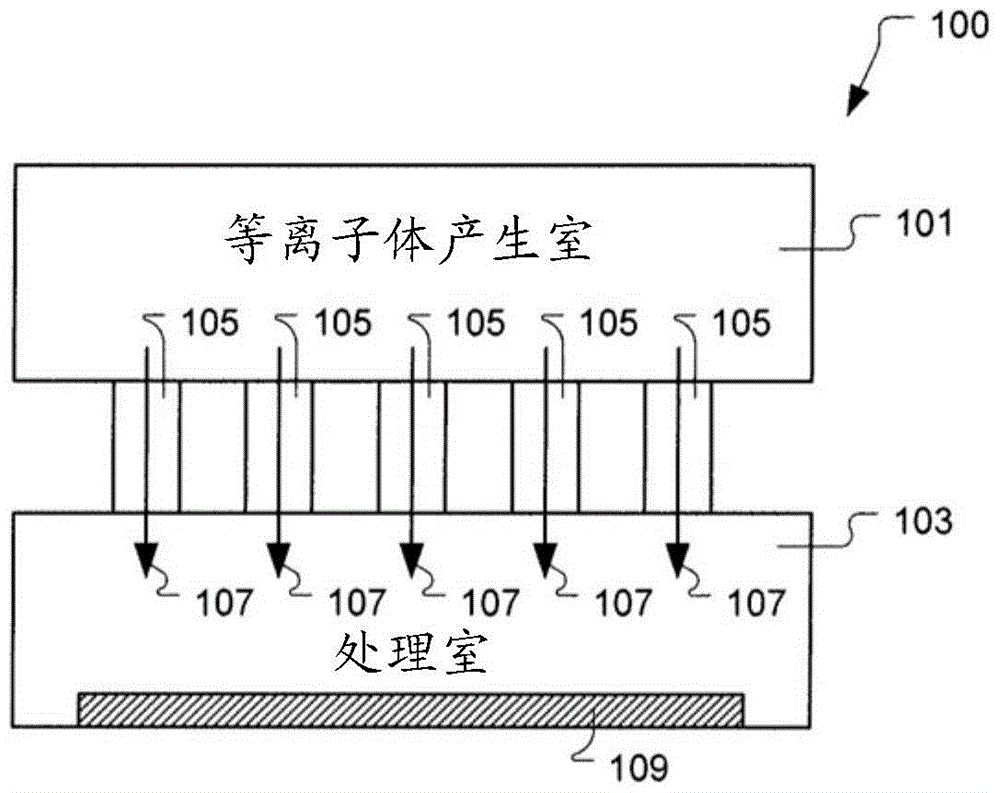
[0030] Plasma sources used for thin film semiconductor processing often cannot achieve optimal conditions for dry etching due to the inability to separately adjust the concentrations of ions and free radicals in the plasma. In many applications, ideal conditions for plasma etching can be achieved by increasing the concentration of ions while maintaining the concentration of free radicals at a substantially constant level. However, achieving such adjustments with conventional plasma sources for thin film processing is difficult at best.

[00...


PUM


Abstract

A semiconductor substrate processing system includes a processing chamber and a substrate support defined to support a substrate in the processing chamber. The system also includes a plasma chamber defined separate from the processing chamber. The plasma chamber is defined to generate plasma. The system also includes a plurality of fluid transfer passages fluidly connecting the plasma chamber and the processing chamber. The plurality of fluid delivery pathways are defined to supply reactive components of the plasma from the plasma chamber to the processing chamber. The system further includes an electron injection device for injecting electrons into the processing chamber to control the energy distribution of the electrons within the processing chamber to thereby control the ion-to-radical density ratio within the processing chamber. In an embodiment, an electron beam source is defined to deliver an electron beam through the process chamber above and across the substrate support.

Description

Background technique [0001] Because the concentration of ions and free radicals in the plasma cannot be controlled separately, the plasma source used for thin film processing in the manufacture of semiconductor devices often cannot achieve the most ideal conditions for dry etching. For example, in some applications, ideal conditions for plasma etching can be achieved by increasing the concentration of ions in the plasma while maintaining the concentration of free radicals at a constant level. However, this independent control of radical concentration and ion concentration cannot be achieved using conventional plasma sources commonly used in thin film processing. Against this background, the present invention has been made. Contents of the invention [0002] In one embodiment, a semiconductor substrate processing system is disclosed. The system includes a processing chamber and a substrate support defined to support a substrate in the processing chamber. The system also in...

Claims


Application Information

Patent Timeline
Patent Type & Authority Patents(China)
IPC IPC(8): H01J37/32B05D3/06B05D3/14
CPCC23F1/08H01L21/3065
Inventor 约翰·帕特里克·霍兰彼得·L·G·温特泽克哈梅特·辛格品川俊越石光
Owner LAM RES CORP
Why Eureka
Try Eureka