Thin film deposition device and thin film deposition method

A thin film deposition device and thin film deposition technology, applied in the field of microelectronics, can solve the problems of increasing the coverage of holes and grooves on the wafer 5, damage to the surface of the wafer 5, etc., and achieve the effects of weakening bombardment, reducing kinetic energy, and reducing negative bias voltage Effect

Active Publication Date: 2016-08-31
BEIJING NAURA MICROELECTRONICS EQUIP CO LTD
View PDF4 Cites 0 Cited by
  • Summary
  • Abstract
  • Description
  • Claims
  • Application Information

AI Technical Summary

Problems solved by technology

This negative bias will attract positive metal ions generated from the target, increasing the coverage of the hole grooves of the wafer 5, and at the same time, the negative bias will attract argon ions to bombard the surface of the wafer 5 and cause re-sputtering. The surface or interface of the wafer 5 is very sensitive to the orientation and epitaxial growth of the crystal plane, which will cause damage to the surface of the wafer 5

Method used


Image

  • Thin film deposition device and thin film deposition method
  • Thin film deposition device and thin film deposition method
  • Thin film deposition device and thin film deposition method

Examples


Embodiment Construction

[0044] In order to enable those skilled in the art to better understand the technical solution of the present invention, the thin film deposition device and thin film deposition method provided by the present invention will be described in detail below with reference to the accompanying drawings.

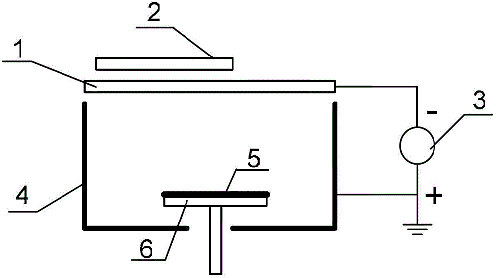
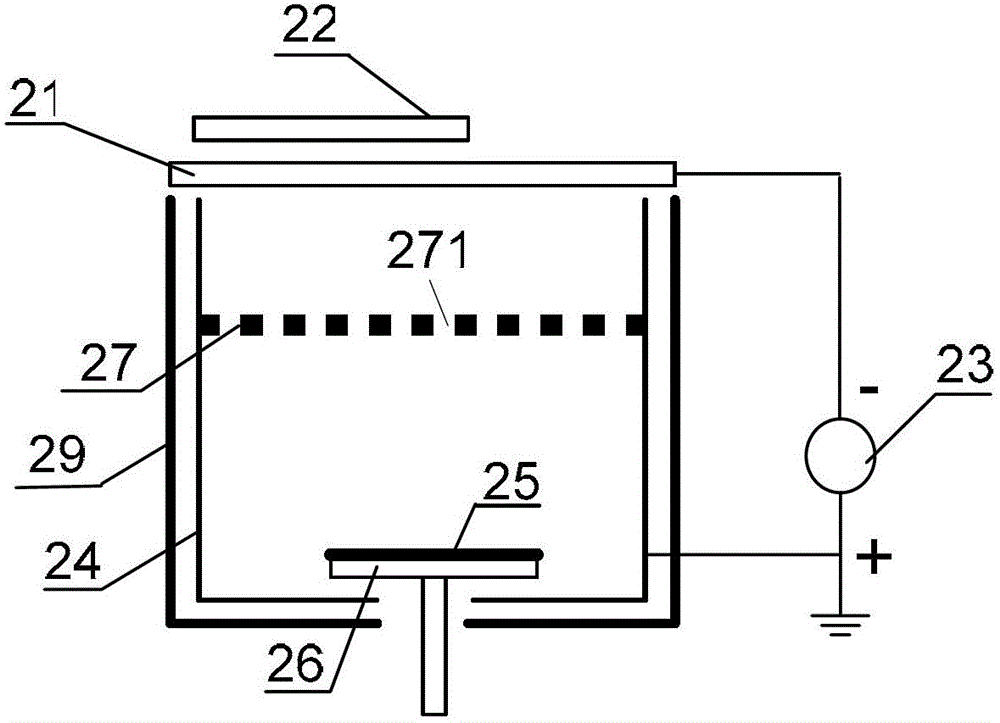
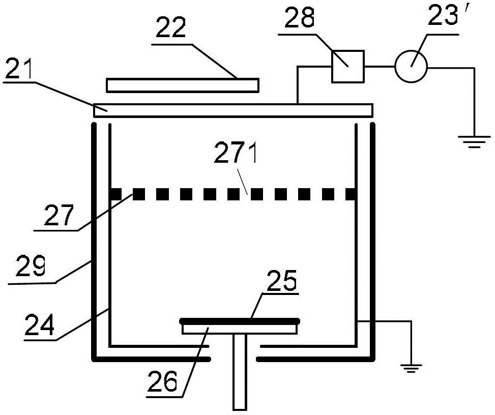
[0045] This embodiment provides a thin film deposition device, figure 2 It is a schematic diagram of a thin film deposition device provided by an embodiment of the present invention. Such as figure 2 As shown, the thin film deposition device includes a reaction chamber 29 , and a target 21 is arranged on the top of the reaction chamber. The target 21 is electrically connected to a power source, and the power source applies a bias voltage to the target 21 . A wafer supporting device 26 is provided at the bottom of the reaction chamber 29 , and the wafer supporting device 26 is opposite to the target 21 . The wafer support device 26 can be a device capable of fixing the wafer such...


PUM

PropertyMeasurementUnit
diameteraaaaaaaaaa

Abstract

The present invention provides a thin film deposition device and a thin film deposition method. The thin film deposition device includes a reaction chamber, a target, a wafer support device, an energy controller, and a power source electrically connected to the target, and the power source is arranged at Outside the reaction chamber, the target is arranged at the top of the reaction chamber, the wafer support device is arranged at the bottom of the reaction chamber and is opposite to the target, and the energy controller is arranged at The target and the wafer supporting device are connected to the ground, and the energy controller is provided with a plurality of through holes penetrating through its thickness, and the inner diameter of the through holes is smaller than the mean free path of molecular collision. The thin film deposition device can reduce the damage on the wafer surface.

Description

technical field [0001] The invention belongs to the field of microelectronics, and relates to a thin film deposition device and a thin film deposition method. Background technique [0002] Physical vapor deposition equipment is often used to form thin films on wafers. figure 1 It is a typical physical vapor deposition equipment. Such as figure 1 As shown, the physical vapor deposition apparatus comprises a reaction chamber having a chamber wall 4 . A target 1 is arranged on the top of the reaction chamber, and a magnetron 2 is arranged above the target 1 . A wafer support device 6 is provided at the bottom of the reaction chamber 1 and opposite to the target 1 , and the wafer support device 6 is in a suspended state (not grounded). Wafer 5 is placed on the upper surface of wafer support device 6 . A DC power supply 3 is also provided outside the reaction chamber 1 , the negative pole of the DC power supply 3 is connected to the target 1 , and the other end of the DC pow...

Claims


Application Information

Patent Timeline
Patent Type & Authority Patents(China)
IPC IPC(8): C23C14/54C23C14/34
Inventor 王厚工丁培军耿波李杨超武学伟
Owner BEIJING NAURA MICROELECTRONICS EQUIP CO LTD
Why Eureka
Try Eureka